


Revision Notes on Semiconductor for NEET 2025 - Free PDF Download
Semiconductors:
Certain substances, like germanium, silicon, etc., have exhibited resistance between excellent conductors like copper and insulators like glass. These substances are referred to as semiconductors.
Semiconductors are substances with resistivities that fall between insulators and conductors. At ambient temperature, a semiconductor's resistivity ranges about between $10^{-2} \text { and } 10^{4} \Omega m$.
Over a certain temperature range, a semiconductor's resistance reduces as temperature rises.
This behaviour contrasts with the behaviour of a metallic conductor, for which the resistance rises as the temperature rises.
The elements classified as semiconductors are Si, Ge, In, etc. Germanium and silicon are most widely used as semiconductors.
Energy Bands in Solid

Energy Band in Solid
Valence Band:
The band created by a series of energy levels including the valence electrons can be defined as the valence band. The valence band can be explained as a band which is inhabited by the valence electrons or a band which is having highest inhabited band energy.
Conduction Band:
The conduction band can be explained as the least unfilled energy band.
Forbidden Energy Gap:
The forbidden energy gap can be defined as the separation between conduction band and valence band. There will be no permitted energy state in this gap and therefore electrons can't occupy the forbidden energy gap.
$\Delta \mathrm{Eg} .=(\mathrm{CB})_{\text {Min }}-(\mathrm{VB})_{\text {Max }}$
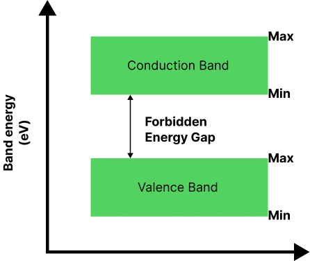
Forbidden Energy Gap
Classification of Solids Based on Forbidden Energy Gap:
Conductors, semiconductors and insulators can be distinguished from one another by the size of the forbidden energy gap between the valence band and conduction band.
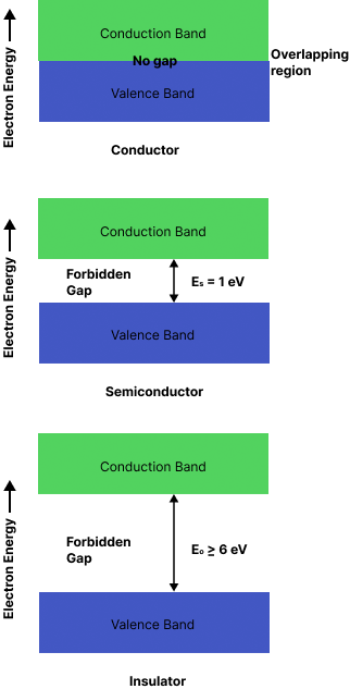
Classification of Solids Based on Forbidden Energy Gap
Comparison Between Conductor, Semiconductor and Insulator:
Types of Semiconductor:
Intrinsic Semiconductor:
The term "intrinsic semiconductors" and "intrinsic conductivity" refer to pure semiconductors whose electrical conductivity is entirely controlled by electrons driven from the valence band to the conduction band and in which no impurity atoms are added to boost their conductivity. Electron-hole pairs conduct electricity in pure semiconductors in an inherent semiconductor.
${n_e} = {n_h} = {n_i}$
where ne = the free electron density in the conduction band, nh = the hole density in the valence band, and ni = the intrinsic carrier concentration.
Extrinsic Semiconductors:
Extrinsic semiconductors are semiconductors that have been doped with the appropriate impurity atoms to boost their conductivity.
Types of Extrinsic Semiconductors:
Extrinsic semiconductors are of two types:
n-type semiconductors
p-type semiconductors
n-type Semiconductors:
Because they give electrons to the host crystal, the pentavalent impurity atoms are known as donors, and the semiconductor doped with donors is an n-type semiconductor. In n-type semiconductors, electrons are the majority charge carriers and holes are the minority charge carriers. Thus,${n_e} > > {n_h}$. Bismuth, antimony, arsenic, phosphorus are examples of n-type semiconductors.
p-type Semiconductors:
Because they produce holes that can accept electrons from adjacent bonds, the trivalent impurity atoms are known as acceptors. A p-type semiconductor has acceptor-type impurities doped into it. In a p-type semiconductor, holes are the majority carriers and electrons are the minority charge carriers Thus,${n_h} > > {n_e}$. Gallium, indium, aluminium, and boron are examples of p-type semiconductors.
Fermi Energy Level:
The highest kinetic energy an electron can have at absolute zero degrees Celsius is known as the fermi energy level, and these electrons are referred to as fermi electrons.
It is always located between the valence band and the conduction band.
The energy known as the Fermi level corresponds to the gravitational centre of the conduction electrons and holes when their energies are weighted.
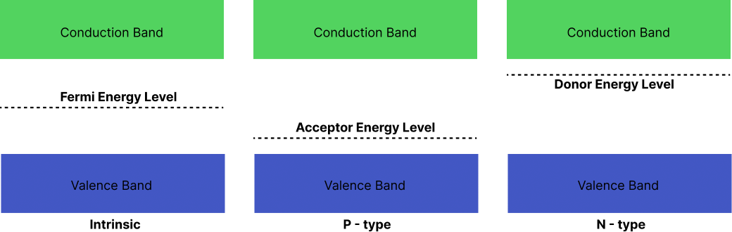
Fermi Energy Level
The fermi level in a pure germanium semiconductor is positioned halfway through the forbidden gap.
The fermi level in an n-type semiconductor is located in the forbidden gap, extremely near to the conduction band.
The fermi level in a p-type semiconductor is located in the forbidden gap, extremely near to the valence band.
For both varieties of semiconductors, the fermi level travels toward the centre of the forbidden gap as the temperature rises.
Because electrons are more mobile than holes, the n-type semiconductor performs better than the p-type semiconductor.
Mass Action Law:
Under thermal equilibrium the product of concentration $\mathbf{n}_{\mathbf{e}}$ of free electrons and the concentration $\mathbf{n}_{\mathbf{h}}$ of holes is constant and independent of the amount of doping by donor and acceptor impurity.
$n_{e} n_{h}=n_{i}^{2} \quad \text { where } n_{i}=\text { intrinsic concentration }$
However, the intrinsic concentration is a function of temperature.
In n-type semiconductors, the number density of electrons is nearly equal to the number density of donor atoms $\mathrm{N}_{\mathrm{d}}$ and is very large as compared to the number density of holes.
$\mathrm{n}_{e} \approx \mathrm{N}_{\mathrm{D}} \quad \mathrm{N}_{\mathrm{D}}>>\mathrm{n}_{\mathrm{h}}$
In p-type semiconductor, the number density of holes is nearly equal to the number density of acceptor atoms $\mathrm{N}_{\mathrm{a}}$ and is very large as compared to the number density of electrons.
$\mathrm{n}_{\mathrm{h}} \approx \mathrm{N}_{\mathrm{A}} \quad \mathrm{N}_{\mathrm{A}}>>\mathrm{n}_{e}$
Holes:
The vacancy or absence of electrons in the bond of a covalently bonded crystal is called a hole. A hole serves as a positive charge carrier.
Mobility:
The drift velocity acquired by a charge carrier in a unit electric field is called its electrical mobility and is denoted by $\mu $.
$\mu = \dfrac{{\left| {{V_d}} \right|}}{E}$
The mobility of an electron in the conduction band is greater than that of the hole (or electron) in the valence band.
PN- junction
A P-N junction is an interface or border between two types of semiconductor material inside a semiconductor, namely the p-type and the n-type.The P-N junction is formed in a semiconductor via the doping method. The semiconductor's p-side, or positive side, has an excess of holes, whereas the n-side, or negative side, has an excess of electrons. The next part goes into greater detail on the doping process.
Formation of P-N Junction
As we all know, when we utilise various semiconductor materials to construct a P-N junction, there will be a grain boundary that will hinder electron flow from one side to the other by scattering electrons and holes, which is why we need the doping procedure.
With the help of this example, we will comprehend the doping process. Take a look at a thin p-type silicon semiconductor sheet. When we add a trace of pentavalent impurity to this, some of the p-type Si is changed to n-type silicon.
This sheet will now have both the p-type and n-type sections, as well as a junction between the two. Following the formation of a P-N junction, two sorts of processes occur: diffusion and drift.
The concentration of holes and electrons differs on opposite sides of a junction. The p-side holes diffuse to the n-side, and the n-side electrons diffuse to the p-side. These cause a diffusion current to flow across the junction.

Formation of P-N Junction
In addition, when an electron diffuses from the n-side to the p-side, an ionised donor remains on the n-side, which is stationary. As the process continues, a layer of positive charge forms on the n-side of the junction.
Similarly, when a hole travels from the p-side to the n-side, an ionised acceptor is left behind on the p-side, creating a layer of negative charges in the junction's p-side.The depletion region is defined as the region of positive and negative charge on either side of the junction.
Because of the positive space charge region on either side of the junction, an electric field is created that points from a positive charge to a negative charge.
An electron on the p-side of the junction goes to the n-side of the junction as a result of the electric field. This is known as drifting.
The direction of the drift current is opposite that of the diffusion current in this case.
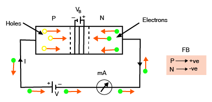
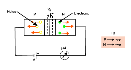
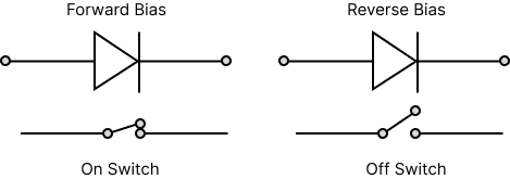
Forward Biasing of a PN-junction:
The PN-junction is referred to as forward-biased if the positive terminal of a battery is connected to the p-side and the negative terminal to the n-side. Both electrons and holes approach the junction. Crossing the junction is a current known as forward current. Thus a PN-junction offers a low resistance when it is forward biased.
Forward Biasing of a PN-junction
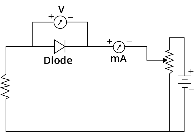
Forward Current Equation of PN Junction Diode
The diode equation is given as
$I_{D}=I_{S}\left(e^{q V_{D} / N k T}-1\right)$
Here,
$I_{D}=$ diode current in amps
$I_{S}=$ Saturation current in amps $\left(1 \times 10^{-12} \mathrm{amps}\right)$
$\mathrm{e}=$ Euler's constant $(\sim 2.718281828)$
$q=$ charge of electron $\left(1.6 \times 10^{-19}\right.$ coulombs $)$
$V_{D}=$ Voltage applied across diode in volts
$\mathrm{N}=$ emission coefficient (between 1 and 2)
$\mathrm{k}=$ Boltzmann's constant $\left(1.38 \times 10^{-23}\right)$
$\mathrm{T}=$ Junction Temperature
The phrase kT/q refers to the voltage produced within the PN junction as a result of temperature, and this temperature is referred to as the thermal voltage. At room temperature, the value of kT/q is equal to 26 millivolts. Let us suppose N is equal to 1. The diode equation can therefore be expressed as
$I_{D}=I_{S}\left(e^{V_{D} / 0.026}-1\right)$
Knee or cut in voltage
$\mathrm{Ge} \rightarrow 0.3 \mathrm{~V}$
$\mathrm{Si} \rightarrow 0.7 \mathrm{~V}$
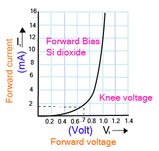
Forward Current graph of PN Junction Diode
Reverse Biasing of a PN-junction:
The PN-junction is reverse biassed if a battery's positive terminal is connected to the n-side and the negative terminal to the p-side. Most charge carriers shift away from the junction. During the reverse bias, the potential barrier presents significant resistance. However, a tiny current known as reverse current or leakage flows in the opposite direction due to the minority charge carriers. Thus the junction diode has almost a unidirectional flow of current.
Reverse Biasing of a PN-junction
Because of minority carrier flow, very little current, known as reverse saturation current, flows.
For Silicon $=10^{-9} \mathrm{~A}$
For Germanium $=10^{-6} \mathrm{~A}$
When reverse biassed, the junction behaves like a few picofarad capacitors.
When reverse biassed, the junction acts like a high resistive substance between two regions.
The $\mathrm{P}-\mathrm{N}$diode behaves like an insulator when reverse biassed.
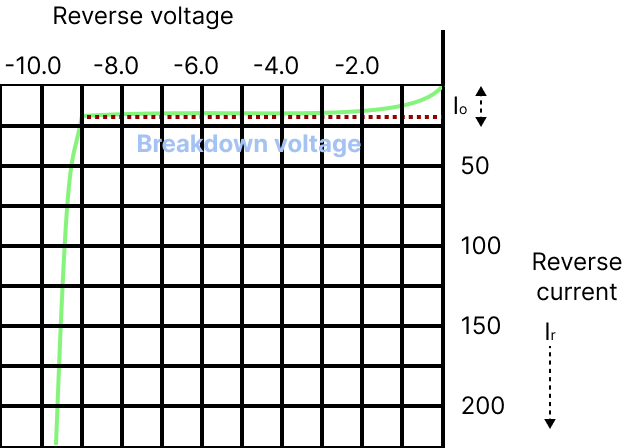
Characteristic Graph of Reverse Biasing of a PN-junction
Reverse resistance $\mathrm{R}_{\mathrm{B}}=\dfrac{\Delta \mathrm{V}_{\mathrm{B}}}{\Delta \mathrm{I}_{\mathrm{B}}} \cong 10^{6} \Omega$
$\dfrac{R_{B}}{R_{f}}=10^{3}: 1$ for $G e \quad$ and $\quad \dfrac{R_{B}}{R_{f}}=10^{4}: 1$ for $\mathrm{Si}$
Dependence of reverse current on bias volt.
$I_{r}=I_{0}\left[e^{-\dfrac{q v}{k T}}-1\right], e^{-\dfrac{q v}{x T}} \ll 1, I \cong-I_{0}$
Here
$I_{r}=$ reverse current
$I_{0}=$ reverse saturation current
V= applied voltage
q= charge of electron
T= temperature in kelvin
Diode
Diode is a PN junction device
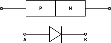
Diode
Ideal Diode
When forward biassed, conduct with zero resistance.
When reverse biassed, they provide infinite resistance.
Ideal Diode
Practical Guide for Diode
Diode
Transistor:
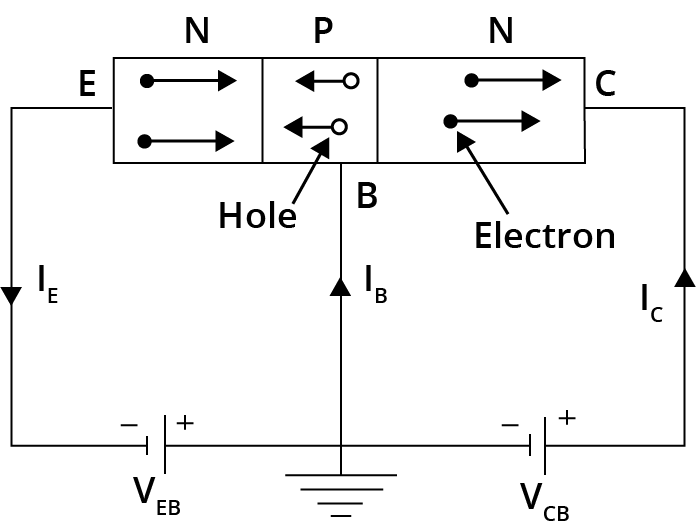
Transistor is used in place of a triode valve; it is an electronic device formed by $\mathrm{P}$ and $\mathrm{N}$ types of semiconductors. Transistor is three terminals and two P-N Jn. device.
Transistor is Three Terminals and Two P-N Jn. Device.
There are two types of transistors
N-P-N transistor and
P-N-P transistor
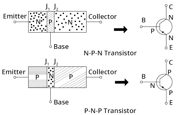
N-P-N Transistor and P-N-P Transistor
A transistor (P-N-P or $\mathrm{N}-\mathrm{P}-\mathrm{N})$ is made up of the following sections:
Emitter: It emits charge carriers and is highly doped.
Base: The base is the centre part of the transistor. This is very lightly doped and very thin $\left(10^{-6} \mathrm{~m}\right)$
Collector: This is moderately doped. It collects the charge carriers
Working:
The positive terminal of the battery $\mathrm{V}_{\mathrm{EE}}$ towards the base fills the holes of the $P$ area (emitter). Because the potential barrier at the emitter junction is decreased due to the forward bias, the holes traverse this junction and penetrate into the$\mathrm{N}$ area. The emitter current is made up of this. Because the base region is very thin and lightly doped, only two to five percent of the holes recombine with the free electrons of the $\mathrm{N}$ region. This is the base current $\mathrm{I}_{B}$, which is, of course, quite little. The remaining holes ($95 percent $ to $98 percent)$ can wander across the base and into the collection region. The collector current is made up of this.
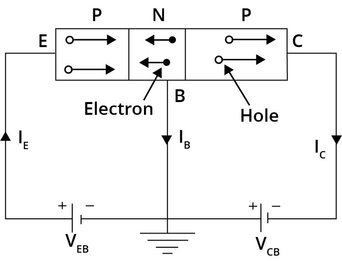
PNP transistor working
N-P-N Transistor:
Working: The electrons in the emitter area are replenished from the battery's negative terminal to the emitter junction. Electrons cross the p-type base area because the potential barrier at the junction is decreased due to forward bias and the base region is very thin and weakly doped. A few electrons mix with holes in the P-region and are lost as charge carriers. The positive collector voltage $V_{c c}$ can now easily sweep up electrons in the N-region (collector region).
NPN Transistor
Transistor Configuration
Three types of transistor circuit configuration are
Common base (CB)
Common emitter (CE)
Common collector (CC)
Common Base Configuration
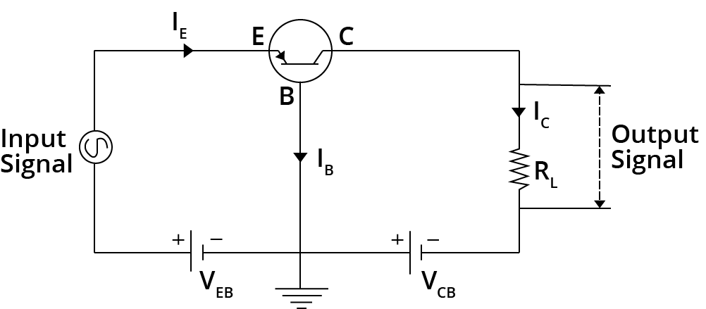
Common Base Configuration
The input signal is applied between the emitter and the base in this design, and the output is obtained from the collector and the base. The phase difference between input and output is zero in the common base as an amplifier.
Input Characteristic :
The curve between emitter current $\mathrm{I}_{E}$ and emitter base voltage $\mathrm{V}_{\mathrm{EB}}$ at constant collector base voltage $\mathrm{V}_{\mathrm{CB}}$ represents the input characteristics. Collector base voltage $V_{C B}$ is kept fixed.
There exists a cut in, offset or threshold voltage $V_{E B}$ below which the emitter current is very small.
The emitter current $\mathrm{I}_{E}$ increases rapidly with a small increase in emitter-base voltage $\mathrm{V}_{\mathrm{EB}}$. This shows that the input resistance is very small.
Output Characteristic :
Curve between collector current $\mathrm{I}_{\mathrm{C}}$ and collector base voltage $\mathrm{V}_{\mathrm{CB}}$ at constant emitter $\mathrm{I}_{\mathrm{E}}$ represents the output characteristic.
Common Emitter Configuration
The input signal is applied between the base and the emitter in this setup, and the output is obtained from the collector and the emitter.
The phase difference between input and output in a common emitter amplifier is $\pi$.
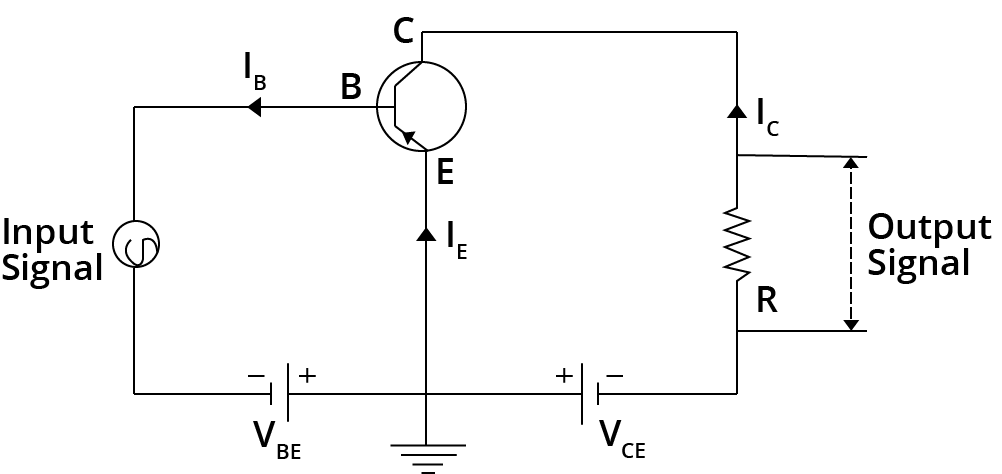
Common Emitter Configuration
Input Characteristics :
The curve between base current $\mathrm{I}_{\mathrm{B}}$ and base emitter voltage $\mathrm{V}_{\mathrm{BE}}$ at constant collector-emitter voltage $\mathrm{V}_{\mathrm{CE}}$ represents the input characteristic.
In this case $I_{B}$ increases less rapidly with $V_{B E}$ as compared to common-base configuration. This shows input resistance of the common-emitter circuit is higher than that of common-base circuit.
Output Characteristic :
The curve between collector current $\mathrm{I}_{\mathrm{C}}$ and collector emitter voltage $\mathrm{V}_{\mathrm{CE}}$ at constant base current $\mathrm{I}_{\mathrm{B}}$ represents the output characteristic.
Relationship between $\alpha, \beta$ and $\gamma$ :
Emitter current $\mathrm{I}_{\mathrm{E}}=\mathrm{I}_{\mathrm{B}}+\mathrm{I}_{\mathrm{C}}$
divide by $I_{C}$ gives, $\dfrac{I_{E}}{I_{C}}=\dfrac{I_{B}}{I_{C}}+1$ or $\quad \dfrac{1}{\alpha}=\dfrac{1}{\beta}+1$
$\beta=\dfrac{\alpha}{1-\alpha}$
Voltage Gain of an Amplifier:
It is defined as-
Voltage gain = Current gain X Resistance gain.
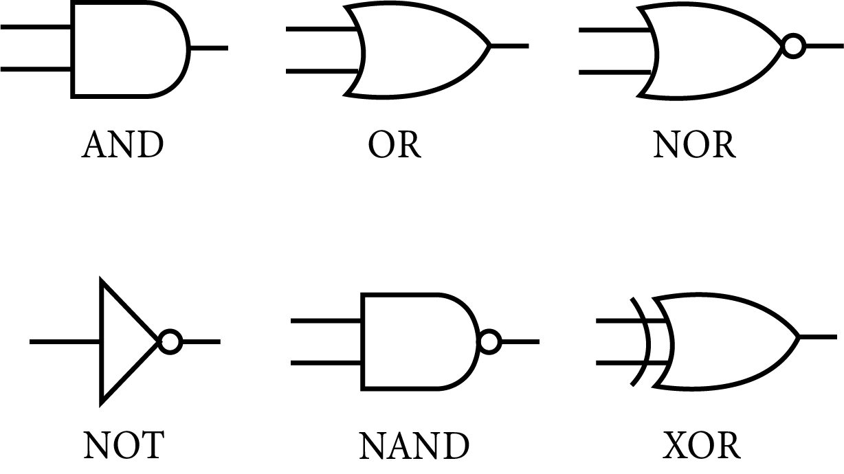
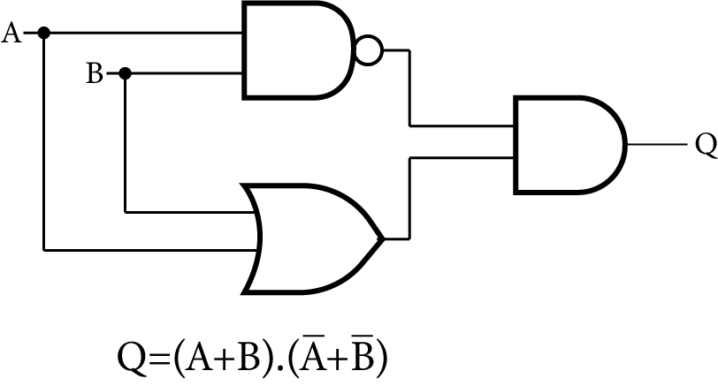
Logic Gate:
A logic gate is a digital circuit that has one or more inputs but only one output. It follows a logical relationship between input and output voltage.
Logic Gate
Truth Table:
This table shows all possible input combinations and the corresponding output for a logic gate.
Truth Table
Boolean Expression:
It is a shorthand method of describing the function of a logic gate in the form of an equation or an expression. It also relates all possible combinations of the inputs of a logic gate to the corresponding output.
Positive and Negative Logic:
If in a system, the higher voltage level represents 1 and the lower voltage level represents 0, the system is called a positive logic. If the higher voltage represents 0 and the lower voltage level represents 1, then the system is called a negative logic.
OR Gate:
An OR gate can have any number of inputs but only one output. It gives a higher output (1) if either input A or B or both are high (1), otherwise, the output is low (0).
A + B = Y
Which is read as ‘A or B equals Y’.
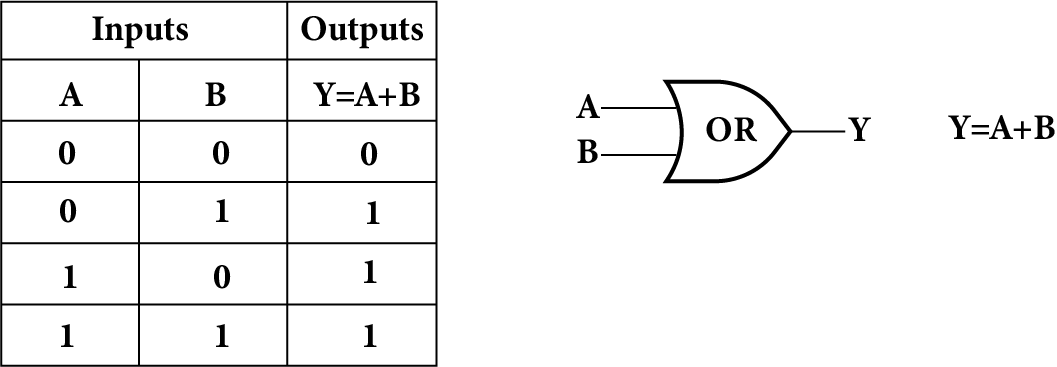
OR Gate
AND Gate:
An AND gate can have any number of inputs but only one output. It gives a high output (1) if inputs A and B are both high (1), or else the output is low (0). It is described by the Boolean expression-
A . B = Y
Which is read as ‘A and B equals Y’.
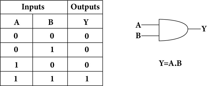
AND Gate
NOT Gate:
A NOT gate is the simplest gate, with one input and one output. It gives a high output (1) if the input A is low (0), and vice versa.
Whatever the input is, the NOT gate inverts it. It is described by the Boolean expression: $Y=\bar{A}$
Which is read as ‘not A equals Y’.
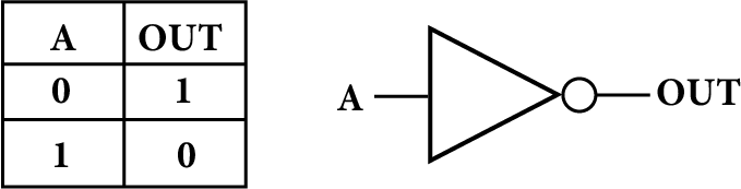
NOT Gate
NAND (NOT + AND) Gate:
It is obtained by connecting the output of an AND gate to the input of a NOT gate. Its output is high if both inputs A and B are not high. If is described by the Boolean expression: $Y=\bar{A.B}$
Which is read as ‘A AND B negated equals Y’.
NOR (NOT + OR) Gate:
It is obtained by connecting the output of an OR gate to the input of a NOT gate. Its output is high if neither input A nor input B is high. It is described by the Boolean expression: $Y=\bar{A + B}$
Which is read as ‘A OR B negated equals Y’.
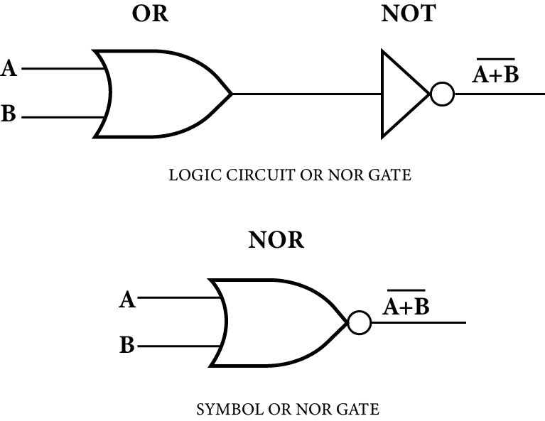
NOR Gate
XOR or Exclusive OR gate:
The XOR gate gives a high output if either input A or B is high but not when both A and B are high or low. It can be obtained by using a combination of two NOT gates, two AND gates, and one OR gate. It is described by the Boolean expression: $\text { A. } \bar{B}+\bar{A} \cdot B$.
The XOR gate is also known as the difference gate because its output is high when the inputs are different.
XOR Gate
Integrated Circuits:
The concept of fabricating an entire circuit (consisting of many passive components like R and C and active devices like diode and transistor) on a small single block (or chip) of a semiconductor has revolutionised electronics technology. Such a circuit is known as Integrated Circuit (IC).
Important Formula:
Common Mistakes Students Make When Studying for Exams
Some of the important topics that are important for NEET point of view are: Energy bands in solids (qualitative ideas only), conductors, insulators and semiconductors; semiconductor diode- I-V characteristics in forward and reverse bias, diode as a rectifier; I-V characteristics of LED, Logic gates.
Logic gates are very much important and direct questions are asked, so while making a table and solving the problem, we should not get confused between the numbers 0 and 1.
After studying the entire chapter, we should dedicate a good amount of time for the revision.
Lack of revision will lead to confusion, it is always better to revise the parts we studied and make a note of it.
Importance of Physics Semiconductor
This chapter is important in the Class 12 Physics NEET syllabus as it covers the scientific principles of semiconductors. It defines how these materials are designed and for what purposes. Semiconductors are different from conductors and insulators. If we concentrate on the name, we can easily understand that the conductance of these materials is in between the insulators and conductors we generally use.
According to this chapter, there are energy bands existing in solids. These bands act differently when coming in close contact with an isolated single atom. Also, the valence shell electrons are not strongly bound in the solids, especially in the conductors. They start moving from one atom to the other when electricity is passed or there is a potential difference.
The intermixing of different permissible energy levels causes variations resulting in different energy levels or bands. With this concept, this chapter will introduce what a conductance band is. It will also explain the forbidden energy gap and the valence band. Using these scientific principles, this chapter will explain what conductors, semiconductors, and insulators are.
According to the Semiconductor notes for NEET, semiconductors have the smallest forbidden band or energy gap among these three substances. Due to its electrical conductance features lying between the insulators and conductors, an insignificant amount of energy can make its electrons jump from the valence band to the conductance band.
On proceeding further, this chapter will establish the concepts of semiconductors using mathematical expressions and pictorial illustrations.
Benefits of Vedantu’s Semiconductor Revision Notes
These revision notes have been designed to provide a simpler explanation of these concepts mentioned in the semiconductor chapter. It will help aspirants like you to grab the basic concept behind the new terms related to semi-conductance and help to prepare this chapter faster.
Get a concise description of all the new terms, derivations, and formulas mentioned in this chapter to revise it faster. There is no need to refer to the pages in your physics textbook when you can use Semiconductor revision notes to complete revision easily and reduce your preparation time.
The easier format of these notes will help you recall what you have studied. It means you can easily solve the problems by remembering the definitions, derivations, formulas, and examples and score well in the exams.
Download Semiconductor Class 12 Notes PDF
Get the free PDF version of these notes today and make your revision sessions more fruitful. Once you are done studying this chapter elaborately, use these notes to trigger your memory and remember everything you have studied. These notes will enable you to prepare and complete your physics syllabus exceptionally before the NEET exam.
NEET Physics Revision Notes - Chapter Pages
Other Important Links

FAQs on Semiconductor Notes for NEET 2025
1. What is a conductor?
A material that allows an electric current to flow with a minimum interruption is called a conductor. Example: Copper, aluminium, gold, etc.
2. What is a non-conductor?
A non-conductor is an insulating material that does not allow the passage of electrons through its constituent atoms and molecules. Example: Bakelite, plastic, porcelain.
3. Name a conducting non-metal.
The best example of a conducting non-metal is graphite. It is an allotrope of carbon that conducts electricity.
4. Name a non-conducting metal.
A non-conducting metal is Bismuth. It does not allow the passage of electrons through it despite being a metal.