


NCERT Exemplar For Class 12 Free PDF Download
Exercise
MULTIPLE CHOICE QUESTIONS - I
14.1 The conductivity of a semiconductor increases with increase in temperature because
number density of free current carrier's increases.
relaxation time increases.
both number density of carriers and relaxation time increase.
number density of current carrier's increases, relaxation time decreases but effect of decrease in relaxation time is much less than increase in number density.
Ans: Option (d)
Because the density of charge carriers (electrons and holes) in semiconductors is very low, the resistance is significant. The density of charge carriers (density) increases as temperature rises, increasing conductivity. The velocity of free electrons increases as the temperature of the semiconductor rises, reducing the relaxation time. Because the charge carrier density is low, the influence on relaxation time is minimal.
14.2 In Fig. 14.1, Vo is the potential barrier across a p-n junction, when no battery is connected across the junction
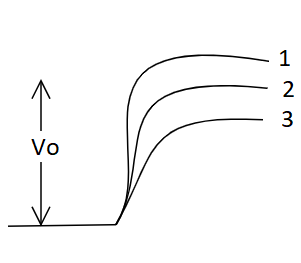
1 and 3 both correspond to forward bias of junction
3 corresponds to forward bias of junction and 1 corresponds to reverse bias of junction
1 corresponds to forward bias and 3 corresponds to reverse bias of junction
3 and 1 both correspond to reverse bias of junction.
Ans: Option (b)
When the P-n junction is in the forward bias, it compresses or reduces the depletion layer, lowering the potential barrier in forward bias and increasing the potential barrier in reverse bias.
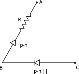
14.3 In Fig. 14.2, assuming the diodes to be ideal,
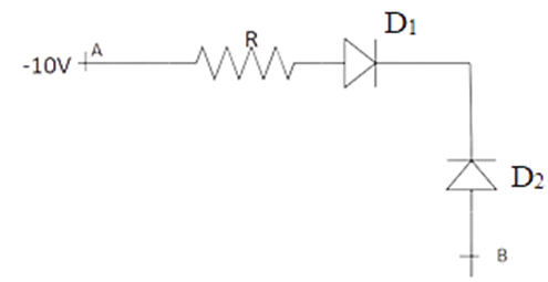
D1 is forward biased and D2 is reverse biased and hence current flows from A to B
D2 is forward biased and D1 is reverse biased and hence no current flows from B to A and vice versa.
D1and D2 are both forward biased and hence current flows from A to B.
D1 and D2 are both reverse biased and hence no current flows from A to B and vice versa.
Ans: Option (b)
A is -10V, and B is 0V in this circuit. As a result, B is more positive and greater than A. As a result of D2's forward bias and D1's reverse bias, there is no flow of current from A to B or B to A.
14.4 A 220 V A.C. supply is connected between points A and B (Fig. 14.3). What will be the potential difference V across the capacitor?
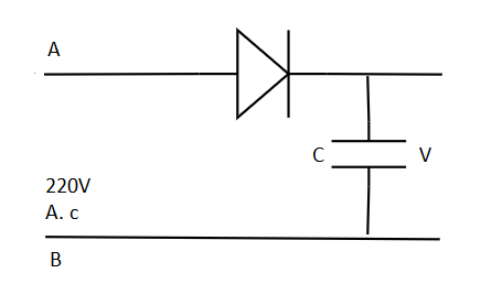
220 V
110 V
0 V
$220\sqrt{2}V$
Ans: Option (d)
When the diode is at forward bias, the potential difference across the capacitor equals the maximum voltage. When end A of the cycle has a positive potential, the diode will be forward biased.
Therefore, the potential at C = Peak value of V = ${{V}_{rms}}\sqrt{2}=220\sqrt{2}V$
14.5 Hole is
an antiparticle of electrons.
a vacancy created when an electron leaves a covalent bond.
absence of free electrons.
an artificially created particle.
Ans: Option (b)
Covalent bonds among atoms of similar or differing types bind semiconductor atoms. When an electron leaves its location and becomes independent due to thermal agitation, it leaves a void in the bond (covalent), which is known as a hole.
14.6 The output of the given circuit in Fig 14.4
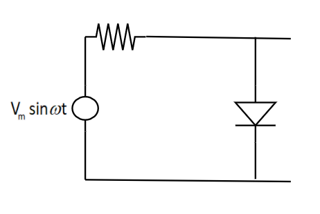
would be zero at all times.
would be like a half wave rectifier with positive cycles in output.
would be like a half wave rectifier with negative cycles in output.
would be like that of a full wave rectifier.
Ans: Option (c)
When the positive cycle is at A, the diode is forward biased, and the resistance owing to the diode is close to zero. Therefore the potential across the diode is close to zero.
Whenever there is a negative half cycle at A, the diode will be in reverse bias, and resistance will be at its highest, resulting in a potential difference across the diode $Vm\text{ }sin~\omega t$ with negative at A. As a result, we only obtain negative output at A, indicating that it functions as a half-wave rectifier with a negative cycle at A in output, confirming the solution (c).
14.7 In the circuit shown in Fig. 14.5, if the diode forward voltage drop is 0.3 V, the voltage difference between A and B is
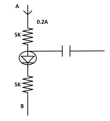
1.3 V
2.3 V
0 V
0.5 V
Ans: Option (b)
The capacitor in the circuit's centre proper functions as an open circuit for d.c 0.2mA current, allowing current to flow exclusively from A to B. Assume that the potential difference between A and B is V, and Kirchhoff's loop law applies,
${{V}_{AB}}=\left( 5000\times 0.2\times {{10}^{-3}} \right)+0.3+5000\times 0.2\times {{10}^{-3}}$
${{V}_{AB}}=1V+0.3V+1V$
${{V}_{AB}}=\text{ }2.3\text{ }V$
14.8 Truth table for the given circuit (Fig. 14.6) is
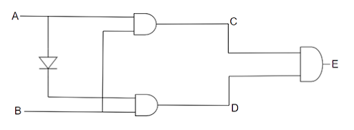
(a)
(b)
(c)
(d)
Ans: Option (c).
Multiple Choice Question: II (More than one option)
14.9 When an electric field is applied across a semiconductor
electrons move from lower energy level to higher energy level in the conduction band.
electrons move from higher energy level to lower energy level in the conduction band.
holes in the valence band move from higher energy level to lower energy level.
holes in the valence band move from lower energy level to higher energy level.
Ans: Options (a) and (c).
The P.E. or electric field energy decreases along the direction of the electric field. As a result, electrons always migrate in the opposite direction of the E.F., i.e. from a lower to an upper energy level. In contrast, holes move from a higher to a lower energy level. Electrons are in the conduction band, while holes are in the valence band in semiconductors.
14.10 Consider an n-p-n transistor with its base-emitter junction forward biased and collector base junction reverse biased. Which of the following statements are true?
Electrons crossover from emitter to collector.
Holes move from base to collector.
Electrons move from emitter to base.
Electrons from the emitter move out of the base without going to the collector.
Ans: Options (a) and (c)
Forward bias connecting emitter to collector repels electrons; 5% of electrons pair with holes in the base, while the rest are repelled. The reverse bias of the collector-base junction attracts 95% of the emitter's electrons.
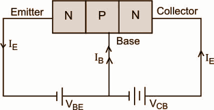
Therefore, the electrons choose the path from emitter to collector via the base which makes option (a) and (c) correct.
14.11 Figure 14.7 shows the transfer characteristics of a base biased C.E. transistor. Which of the following statements are true?
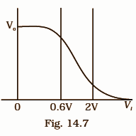
At Vi = 0.4V, the transistor is in an active state.
At Vi = 1V, it can be used as an amplifier.
At Vi = 0.5V, it can be used as a switch turned off.
At Vi = 2.5V, it can be used as a switch turned on.
Ans: Options (b), (c), and (d)
There is no collector current when ${{V}_{i}}=0.4V$ the only output voltage is due to the ${{V}_{ce}}$ battery. As a result, the transistor is not really in active mode at 0.4V.
the transistor is between the active and inactive regions when ${{V}_{i}}=1Volt$ (0.6 V to 2V). As a result, it may be utilized as a power amplifier.
The transistor is in a cut-off condition at ${{V}_{i}}=0.5V$ and can be utilised as an off switch.
The transistor is out of the active area at ${{V}_{i}}=0.25V$ . The collector current is saturated, therefore adjusting the input voltage has no impact, and the transistor may be utilised as a switch switched on.
Therefore, Options (b), (c), and (d) are correct.
14.12 In a n-p-n transistor circuit, the collector current is 10mA. If 95 per cent of the electrons emitted reach the collector, which of the following statements are true?
The emitter current will be 8 mA.
The emitter current will be 10.53 mA.
The base current will be 0.53 mA.
The base current will be 2 mA.
Ans: Options (b) and (c)
Given:
In the n-p-n transistor circuit,
${{I}_{E}}$= Emitter current
${{I}_{C}}=Collector\text{ current = }10mA$
${{I}_{B}}=\text{ Base current}$
Also,
${{I}_{C}}=95%\text{ of }{{I}_{E}}$
${{I}_{C}}=\dfrac{95}{100}\times \text{ }{{I}_{E}}$
${{I}_{E}}=\dfrac{100\times {{I}_{C}}}{95}$
${{I}_{E}}=\dfrac{100\times 10mA}{95}$
${{I}_{E}}=10.53mA$
We know that, ${{I}_{E}}$ is the sum of ${{I}_{C}}$ and ${{I}_{B}}$
$\therefore {{I}_{E}}={{I}_{C}}+{{I}_{B}}$
${{I}_{B}}={{I}_{E}}-{{I}_{C}}$
${{I}_{B}}=10.53-10=0.53mA$
Thus, both option (b) and (c) are correct.
14.13 In the depletion region of a diode
there are no mobile charges
equal number of holes and electrons exist, making the region neutral.
recombination of holes and electrons has taken place.
immobile charged ions exist.
Ans: Options (a), (b), (c) and (d)
When a P-n junction is formed, electrons on the n side and holes on the p side migrate towards each other, forming a potential barrier across the junction. Some holes and electrons or ions cannot travel within the barrier. So there are no roaming charges in the depletion layer, but there are negative and positive ions; when the n-p-n junction developed, the barrier layer was generated by recombination of electrons and holes.
14.14 What happens during the regulation action of a Zener diode?
The current in and voltage across the Zener remains fixed.
The current through the series Resistance ($R_s$) changes.
The Zener resistance is constant.
The resistance offered by the Zener diode changes.
Ans: Options (b) and (d)
The current $R_s$ fluctuates throughout regulation, and the resistance supplied by the Zener diode varies. The current flowing through the Zener diode varies, but the voltage across it does not.
14.15 To reduce the ripples in a rectifier circuit with capacitor filter
R.L. should be increased.
input frequency should be decreased.
input frequency should be increased.
capacitors with high capacitance should be used.
Ans: Options (a), (c) and (d)
The ratio of the r.m.s. the value of the ripple voltage to the absolute value of the D.C. component of the output voltage is known as the ripple factor. It is commonly stated as a percentage. However, the maximum value of ripple voltage is also widely used.
Ripple factor is given by,
$r=\dfrac{1}{4\sqrt{3}\upsilon {{R}_{_{L}}}{{C}_{V}}}$
$\therefore r\propto \dfrac{1}{{{R}_{L}}}$, $r\propto \dfrac{1}{{{C}_{v}}}$ and$r\propto \dfrac{1}{\upsilon }$
${{R}_{L}}$, ${{C}_{v}}$ and $\upsilon $ are in inverse proportion to the ripple factor.
${{R}_{L}}$ should be elevated, input frequency ($\upsilon $) should be increased, and capacitance ${{C}_{v}}$ should be increased to minimise r.
14.16. The breakdown in a reverse biased p–n junction diode is more likely to occur due to
large velocity of the minority charge carriers if the doping concentration is small.
large velocity of the minority charge carriers if the doping concentration is large.
strong electric field in a depletion region if the doping concentration is small.
strong electric field in the depletion region if the doping concentration is large.
Ans: Options (a) and (d)
Due to the strong electric field generated in reverse biasing, minority charge carriers accelerate (due to reverse Potential difference). Consequently, the minority charge carrier in both junctions rushed toward the depletion layer, which, when struck by atoms, produces ionisation, resulting in the secondary electron. So more charge carriers equal more significant current in the opposite direction. The intense doping and many ions in the depletion layer cause a strong electric field across the junction, resulting in much more current in the thin depletion layer.
VERY SHORT ANSWER TYPE QUESTIONS
14.17. Why are elemental dopants for Silicon or Germanium usually chosen from group 13th or group 15th?
Ans: The dopant atom's size should be comparable to that of Si or Ge. So that the geometry of pure Si or Ge is not disrupted, and dopants can donate charge carriers to the formation of covalent bonds between Si or Germanium atoms. Because silicon and germanium belong to the 14th group, their atom sizes will be comparable in the 13th and 15th groups of the modern periodic table.
14.18. Sn, C, and Si, Ge are all group XIV elements. Yet, Sn is a conductor, C is an insulator while Si and Ge are semiconductors. Why?
Ans: If there is no energy gap between the conduction and valence bands in an atom's energy band diagram, the material will transmit current. This energy gap narrows when the material transitions from insulator to semiconductor and then to the conductor. In terms of atomic size, the energy gaps in Sn, Si, C, and Ge are 0 eV, 1.1 Ev, 0.54 eV, and 0.7 eV, respectively. Thus, Si and Ge are semiconductors, Sn is a conductor, while C is an insulator.
14.19 Can the potential barrier across a p-n junction be measured by simply connecting a voltmeter across the junction?
Ans: We cannot calculate the potential barrier across the p-n junction by the voltmeter. The resistance across the depletion layer is smaller than the resistance of the voltmeter, so the current to estimate the potential will not flow in the voltmeter, and the current passes via the junction.
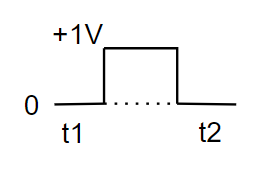
14.20 Draw the output waveform across the resistor (Fig.14.8).
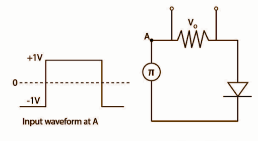
Ans: In the provided circuit, the waveform generated across the resistance diode conducts when the diode is forward biased; hence the output will be only when the input is +1V between $t_1$ and $t_2$. As a result, the output waveform will be between $t_1$ to $t_2$, as shown in the diagram.
14.21 The amplifiers X, Y and Z are connected in series. If the voltage gains of X, Y and Z are 10, 20 and 30, respectively and the input signal is 1 mV peak value, then what is the output signal voltage (peak value)
(i) if the dc supply voltage is 10V?
Ans: The voltage gains of X, Y and Z will be represented by ${{A}_{Vx}}$ , ${{A}_{Vy}}$ and ${{A}_{Vz}}$ respectively. If the D.C. source voltage is 10 V and the output voltage is 6V, the output will be 6V since the theoretical and actual gains are equivalent. Input and output signal voltage will be ${{V}_{i}}$ and ${{V}_{o}}$ respectively.
Given:
${{A}_{Vx}}$= 10
${{A}_{Vy}}$= 20
${{A}_{Vz}}$= 30
${{V}_{i}}$= 1mV = ${{10}^{-3}}V$
We know that,
${{A}_{v}}=\dfrac{{{V}_{o}}}{{{V}_{i}}}$
${{A}_{Vx}}\times {{A}_{Vy}}\times {{A}_{Vz}}=\dfrac{{{V}_{o}}}{{{V}_{i}}}$
${{V}_{o}}={{V}_{i}}\times {{A}_{Vx}}\times {{A}_{Vy}}\times {{A}_{Vz}}$
${{V}_{o}}={{10}^{-3}}V\times 10\times 20\times 30=6000\times {{10}^{-3}}V=6V$
(ii) if dc supply voltage is 5V?
Ans: The output peak cannot surpass 5V when the D.C. supply voltage is 5V or ${{V}_{ce}}=5V$ . As a result, the output voltage will be 5V.
${{V}_{o}}=5V$
14.22 In a C.E. transistor amplifier there is a current and voltage gain associated with the circuit. In other words, there is a power gain. Considering power, a measure of energy, does the circuit violate conservation of energy?
Ans: The DC supply is linked to the C.E. transistor amplifier to provide energy to the signal. As a result, the C.E. the configuration amplifier has a significant power increase. As a result, the output signal's energy equals the sum of the signal's (low) Energy and the Energy supplied by the D.C. source in the output C.E. circuit (Vce).
In the C.E. transistor amplifier, the D.C. supply is connected to give energy to the signal. Owing to this fact, there is a large power gain in the C.E. configuration amplifier. So, the energy of the output signal is equal to the sum of Energy of signal (low) and Energy supplied by the D.C. source in the output C.E. circuit (Vce).
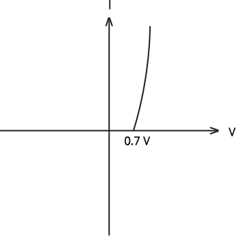
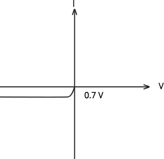
14.23 (i) Name the type of a diode whose characteristics are shown in Fig. 14.9 (a) and Fig. 14.9(b).
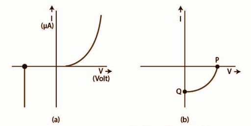
Ans: The diode in fig. (a) shows the characteristics of the Zener diode and the curve in fig. (b) represents a solar cell.
(ii) What does the point P in Fig. (a) represent?
Ans: The point P in fig. (a) represents Zener breakdown voltage.
(iii) What are the points P and Q in Fig. (b) represent?
Ans: Point Q stands for zero voltage and negative current in figure (b). It means that light energy falling on a solar cell with at least a minimal threshold frequency produces a current that is the polar opposite of the current produced by a battery linked to the solar cell. On the other hand, the battery is short-circuited at point P and so represents the short-circuited current.
Point P in figure (b) represents a positive voltage on a solar cell with no current flowing through it.
14.24 Three photo diodes D1, D2 and D3 are made of semiconductors having band gaps of 2.5eV, 2eV and 3eV, respectively. Which ones will be able to detect light of wavelength 6000 ${{A}^{o}}$?
Ans: Given:
$\lambda =6000{{\alpha }^{o}}=6000\times {{10}^{-10}}m$
The formula gives energy of the light photon:
$E=\dfrac{hc}{\lambda }$
Where,
E = energy of light photon
h = Planck’s constant = $6.626\times {{10}^{-34}}~Js$
c = speed of the light = c = $3\times {{10}^{8}}m/s$
λ = wavelength of the light.
$\therefore E=\dfrac{hc}{\lambda }=\dfrac{6.626\times {{10}^{-34}}~\times 3\times {{10}^{8}}}{6000\times {{10}^{-10}}\times 1.6\times {{10}^{-19}}}eV$
$E=\dfrac{6.626\times 3\times {{10}^{-34+8+10+19}}~}{6000\times 1.6}eV$
$E=\dfrac{3.313~}{1.6}eV$
$E=2.06\text{ }eV$
The incident radiation will be detected by the D2 photodiode, as the incident radiation energy is more than the bandgap.
14.25 If the resistance $R_1$ is increased (Fig.14.10), how will the readings of the ammeter and voltmeter change?
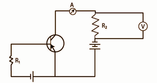
Ans: The change in the reading of the E-C circuit output is given by the following figure:
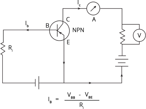
The base current ( ${{I}_{B}}$ )is the ratio of the difference between ${{V}_{BB}}$ and ${{V}_{BE}}$ to the resistor ${{R}_{1}}$. This means the base current ${{I}_{B}}$ is inversely proportional to ${{R}_{1}}$.
So, if ${{I}_{B}}$ will increase ${{R}_{1}}$ will decrease and vice versa.
The collector current (${{I}_{C}}$) is now the current in the ammeter.
I.C. =βIB as I.B. is decreased, I.C. is also decreased, and the reading of voltmeter and ammeter also decreased.
As ${{I}_{B}}$ decreases ${{I}_{C}}=\text{ }\beta {{I}_{B}}$, so, ${{I}_{C}}$ decreases, and the readings on the voltmeter and ammeter decrease as well.
14.26 Two car garages have a common gate which needs to open automatically when a car enters either of the garages or cars enter both. Device a circuit that resembles this situation using diodes for this situation.
Ans: When a car enters one or both of the garages, the common gate automatically opens.
This indicates that if any one of the inputs is high, the output will be high; otherwise, the output will be low.
The device is depicted as follows:
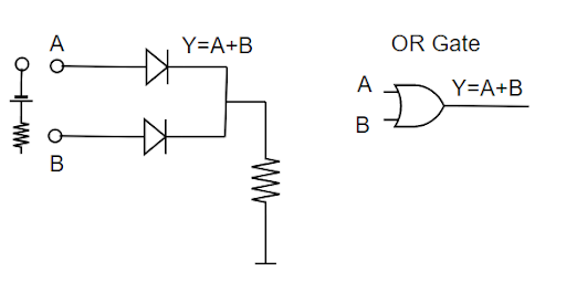
Hence, the OR gate delivers the expected output.
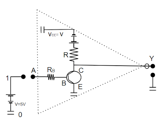
14.27 How would you set up a circuit to obtain NOT gate using a transistor?
Ans: The NOT gate is a device with only one input and outputs each, such as Y = $\overline{A}$ , which indicates Y equals NOT A.
Thus, the truth table will be given by,
The transistor's base B is linked to the input A through the input resistance R.B. The emitter is grounded. A 5V battery is used to power the collector. The voltage at C w.r.t. earth is the output Y.
The resistances R.B. and R.C. are selected so that if the emitter-base junction is unbiased, the transistor is in cut-off mode. If the emitter-base junction is forward biased by 5V input at A, the transistor is in saturation mode.
14.28 Explain why elemental semiconductor cannot be used to make visible LEDs
Ans: The bandgap in an elemental conductor is such that the emissions are infrared rather than visible.
14.29 Write the truth table for the circuit shown in Fig.14.11. Name the gate that the circuit resembles.
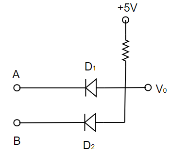
Ans: The circuit is similar to the AND gate. The Boolean expression of the circuit is ${{V}_{0}}=A.B$ , i.e., ${{V}_{0}}$ is equal to A AND B.
The truth table of the gate is shown below:
14.30 A Zener of power rating 1 W is to be used as a voltage regulator. If Zener has a breakdown of 5V and it has to regulate voltage which fluctuates between 3V and 7V, what should be the value of Rs for safe operation (Fig.14.12)?
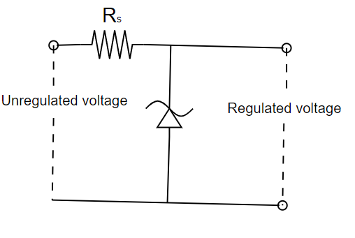
Ans: Given:
P =1 W
Zener breakdown voltage = ${{V}_{z}}$ = 5V
Minimum voltage Vmin = 3 V
Maximum voltage Vmax = 7 V
The formula for power is,
P = VI
${{I}_{{{z}_{\max }}}}=\dfrac{P}{{{V}_{Z}}}=\dfrac{1W}{5V}=0.2A$
Let's calculate the value of Rs,
${{R}_{s}}=\dfrac{{{V}_{\max }}-{{V}_{z}}}{{{I}_{{{z}_{\max }}}}}$
${{R}_{s}}=\dfrac{7-3}{0.2}=20\Omega $
The value of Rs for safe operation is $20\Omega $.
LONG ANSWER TYPE QUESTIONS
14.31 If each diode in Fig. 14.13 has a forward bias resistance of 125Ω and infinite resistance in reverse bias, what will be the values of the current ${{I}_{1}}$ , ${{I}_{2}}$ , ${{I}_{3}}$ and ${{I}_{4}}$ ?
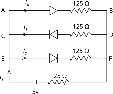
Ans: D1 and D3 diodes are in forward bias and D2 is in reverse bias.
Resistance in-branch A.B. and CD be R1 and R2, respectively.
Hence, resistance in branch AB and EF will be = 125 + 25 = 150 Ω.
Also, resistance in-branch CD is infinite. So, the current in ${{I}_{3}}$ will be zero, i.e. ${{I}_{3}}=0\text{ }\Omega $
So effective resistance (R') will be,
$\dfrac{1}{{{R}^{'}}}=\dfrac{1}{{{R}_{1}}}+\dfrac{1}{{{R}_{2}}}=\dfrac{1}{150}+\dfrac{1}{150}=\dfrac{2}{250}=75\text{ }\Omega $
$Current\text{ }{{I}_{1}}\text{ = }\dfrac{V}{{{R}^{'}}}=\dfrac{5}{100}=0.05A$
As per Kirchhoff’s law,
${{I}_{1}}={{I}_{2}}+{{I}_{4}}+{{I}_{3}}$
But, ${{I}_{3}}=0\text{ }\Omega $
${{I}_{1}}={{I}_{2}}+{{I}_{4}}$
Also, R1 and R2 are equal, so ${{I}_{2}}$ and ${{I}_{4}}$will be equal.
${{I}_{1}}=2{{I}_{2}}$
${{I}_{2}}=\dfrac{{{I}_{1}}}{2}=\dfrac{0.05}{2}=0.025A$
${{I}_{4}}=0.025A$
Therefore, ${{I}_{1}}=0.05A$ , ${{I}_{2}}=0.025A$ , ${{I}_{3}}=0A$ and ${{I}_{4}}=0.025A$.
14.32 In the circuit shown in Fig.14.14, when the input voltage of the base resistance is 10V, Vbe is zero, and Vce is also zero. Find the values of I.B., I.C. and β.
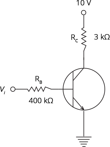
Ans: Voltage across ${{R}_{B}}=10V$
${{V}_{B}}={{R}_{B}}{{I}_{B}}$
${{I}_{B}}=\dfrac{{{V}_{B}}}{{{R}_{B}}}=\dfrac{10}{400\times 1000}A=2.5\times {{10}^{-5}}A$
${{I}_{B}}=25\times {{10}^{-6}}A$
Similarly,
${{I}_{C}}=\dfrac{{{V}_{C}}}{{{R}_{C}}}=\dfrac{10}{4\times 1000}A=3.3\times {{10}^{-3}}A$
Now,
The current gain ($\beta $) will be given by,
$Current\text{ }gain\text{ }(\beta )\text{ = }\dfrac{{{I}_{C}}}{{{I}_{B}}}=\dfrac{3.3\times {{10}^{-3}}}{25\times {{10}^{-6}}}=133$
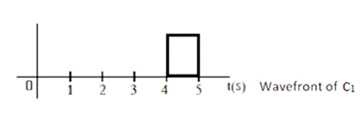
14.33 Draw the output signals C1 and C2 in the given combination of gates (Fig. 14.15).
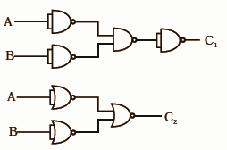
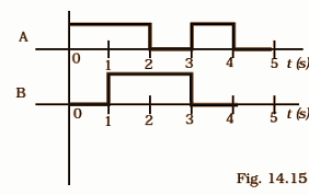
Ans: We can break and draw the recombination circuit as follows:
Circuit for C1:
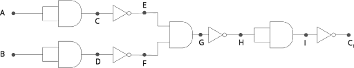
The truth table for the C1 circuit will be a follows:
The wavefront for C1 is drawn below:
Circuit for C2:
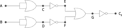
The truth table for the C2 circuit will be a follows:
The wavefront for C2 is drawn below:

14.34 Consider the circuit arrangement shown in Fig 14.16 (a) for studying input and output characteristics of n-p-n transistors in C.E. configuration.
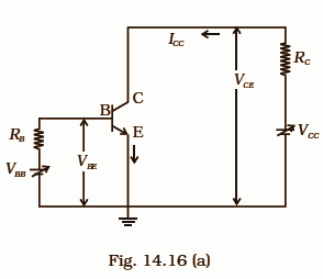
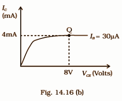
Select the values of R.B. and R.C. for a transistor whose ${{V}_{BE}}=\text{ }0.7\text{ }V$ , so that the transistor is operating at point Q as shown in the characteristics shown in Fig. 14.16. (b) Given that the input impedance of the transistor is minimal and ${{V}_{BB}}={{V}_{CC}}=\text{ 16}V$ , also find the voltage gain and power gain of the circuit making appropriate assumptions.
Ans: At point Q,
VCE = 8V
${{I}_{B}}=\text{ }30\mu A\text{ }=\text{ 30}\times \text{1}{{\text{0}}^{-6}}A$
${{I}_{C}}=\text{ }4mA\text{ }=\text{ 4}\times \text{1}{{\text{0}}^{-3}}A$
VBE = 0.7V
VCC = VBB = 16V
We know that,
${{V}_{CC}}={{I}_{C}}{{R}_{C}}+{{V}_{CE}}$
${{R}_{C}}=\dfrac{{{V}_{CC}}-{{V}_{CE}}}{{{I}_{C}}}$
${{R}_{C}}=\dfrac{16-8}{0.004}=\dfrac{8\times 1000}{4}=2k\Omega $
Similarly,
${{V}_{BB}}={{I}_{B}}{{R}_{B}}+{{V}_{BE}}$
${{R}_{B}}=\dfrac{{{V}_{BB}}-{{V}_{BE}}}{{{I}_{B}}}$
${{R}_{B}}=\dfrac{16-0.7}{30\times {{10}^{-6}}}=510\times {{10}^{3}}=510\text{ }k\Omega $
Now, the current gain is the ratio of I.C. and I.B.,
$\beta =\dfrac{{{I}_{C}}\text{ }}{{{I}_{B}}}=\dfrac{4\times {{10}^{-3}}}{3\times {{10}^{-6}}}=133$
Voltage gain is the product of current gain and the ratio of Rc and R.B.,
$Voltage\text{ }gain\text{ }=\beta \dfrac{{{R}_{c}}}{{{R}_{B}}}=\dfrac{133\times 2\times {{10}^{3}}}{510\times {{10}^{3}}}=0.52$
Power gain is the product of voltage gain and current gain.
$Power\text{ }gain=\beta \times Voltage\text{ gain = 133}\times 0.52=69$
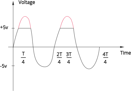
14.35 Assuming the ideal diode, draw the output waveform for the circuit given in Fig. 14.17. Explain the waveform.
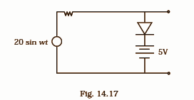
Ans: If the signal 20 $sin\omega t$ provides an input voltage less than 5 volts (because after 5 volts, the diode will receive a positive voltage at its P-junction), the diode will be in reverse bias, and the resistance of the diode will remain infinity, preventing the input signal from passing through the diode and battery path, resulting in an increase in output across A and B from 0 to 5 volts (graph O.C.).
When the input voltage 20 $sin\omega t$ exceeds 5V, the path of the diode 5 V battery offers meagre resistance, allowing current to travel through the diode and battery while keeping the output (across A and B) at 5V. (graph CD). When the voltage drops, the diode will be in reverse bias, and the output will drop from 5 to 0V as the input changes (graph D.E.).
When the input voltage becomes negative (opposite of a 5V battery in a p-n junction, the input voltage develops more than 5V now), the diode is in reversed bias. The output across A.B. will be similar to the input A.C., i.e. for negative cycle diodes offer infinite resistance compared to R in series graphs E, F, and G.
The input and output waveforms are repeated in the graph, which shows the output of the waveform.
14.36 Suppose a 'n’-type wafer is created by doping Si crystal having $5\text{ }\times \text{ }{{10}^{28}}atoms/{{m}^{3}}$ with 1ppm concentration of As. On the surface 200 ppm Boron is added to create the 'P' region in this wafer. Considering ${{n}_{i}}\text{ }=\text{ }1.5\text{ }\times \text{ }{{10}^{16}}{{m}^{-3}}$ , (i) Calculate the densities of the charge carriers in the n & p regions. (ii) Comment which charge carriers would contribute largely for the reverse saturation Current when the diode is reverse biased.
Ans: The n-type water is created when As (pentavalent) is added to Si. As a result, in n-type water, the number of majority carriers is
${{N}_{e}}\text{ }=\text{ }\left( {{N}_{D}}\text{ }and\text{ }{{D}_{Si}} \right)=10\times \text{ }{{10}^{-6}}5\text{ }\times \text{ }{{10}^{28}}atoms/{{m}^{3}}=5\times \text{ }{{10}^{22}}/{{m}^{3}}$
Let's calculate the number of minority carriers,
${{n}_{h}}=\dfrac{{{n}_{i}}^{2}}{{{n}_{e}}}=\dfrac{{{\left( 1.5\times {{10}^{16}} \right)}^{2}}}{5\times {{10}^{22}}}=0.45\times {{10}^{16}}/{{m}^{3}}$
When trivalent boron is placed in Si crystal, a p-type wafer with many holes is generated.
${{n}_{h}}\text{ }=\left( {{N}_{D}}\text{ }\times \text{ }n\text{ }of\text{ }Si \right)\text{ }$
$=\text{ 200}\times {{10}^{-6}}\times 5\times {{10}^{28}}=1\times {{10}^{25}}/{{m}^{3}}$
p-type wafers consist of minority carriers,
${{n}_{e}}=\dfrac{{{n}_{i}}^{2}}{{{n}_{h}}}=\dfrac{{{\left( 1.5\times {{10}^{16}} \right)}^{2}}}{1\times {{10}^{25}}}=2.25\times {{10}^{7}}/{{m}^{3}}$
When a reversed bias is applied to a p-n junction, the minority charge carrier (holes from the n and p sides ${{n}_{e}}=2.25\times {{10}^{7}}/{{m}^{3}}$) travels toward the depletion layer, thickening the depletion layer.
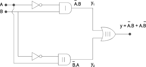
14.37 An X-OR gate has following truth table:
It is represented by the following logic relation $Y=\overline{A}~\cdot B+A\cdot \overline{B}$ . Build this gate using AND, OR and NOT gates.
Ans: As per the problem, the logic relation for the $Y=\overline{A}~\cdot \text{ B}+\text{A}\cdot \overline{B}={{\text{Y}}_{1}}{{Y}_{2}}$ given truth table is
Y1, can be obtained as the output of AND gate I for which one input is through A through NOT gate and another input is of B. Y₂ can be obtained as an output of AND gate Il for which one input is of A and other input is of B through NOT gate. Now, Y1 can be obtained as output from the OR gate, where Y1 and Y₂ are inputs of the OR gate.
The logic relation is expressed as,
14.38 Consider a box with three terminals on top of it as shown in Fig.14.18 (a):
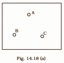
Three components namely, two germanium diodes and one resistor are connected across these three terminals in some arrangement. A student performs an experiment in which any two of these three terminals are connected in the circuit shown in Fig. 14.18 (b).
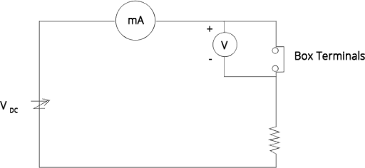
The student obtains graphs of current-voltage characteristics for unknown combinations of components between the two terminals connected in the circuit.
The graphs are:
From these graphs of current – voltage characteristics shown in Fig. 14.18 (c) to (h), determine the arrangement of components between A, B and C.
(i) when A is positive and B is negative

(ii) when A is negative and B is positive
(iii) When B is negative and C is positive
(iv) When B is positive and C is negative
(v) When A is positive and C is negative
(vi) When A is negative and C is positive
Ans: The following are the V-I properties of these graphs:
A reverse characteristic is seen in fig. 1 in the V-I graph of condition I (c). With a resistance in series, A is linked to the n-side of the p-n junction I, and B is linked to the top-side of the p-n junction I.
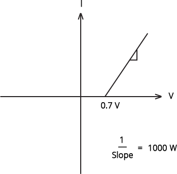
A forward characteristic is displayed in fig. (d) in the V-I graph of condition (ii), where 0.7 V makes the knee voltage of p-n junction I.
$\text{slope}=\dfrac{1}{1000}\Omega$It indicates that A is linked to the n-side of the p-n junction I, B is connected to the p-side of the p-n junction I, and resistance R is in series between A and B on the p-n junction I.
Figure (e) depicts a forward characteristic in the V-I graph of condition (iii), where 0.7 V is the knee voltage. In this example, the p-side of p-n junction II is linked to C, and the n-side of p-n junction II is connected to B.
The connection described above of p-n junctions I and II, as well as a resistance R, is concluded in V-I graphs of conditions (iv), (v), (vi).
As a result, the p-n I, p-n II, and resistance R between A, B, and C will be organized as illustrated in the diagram.
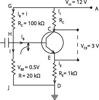
14.39 For the transistor circuit shown in Fig.14.19, evaluate VE, RB, RE given IC = 1 mA, VCE = 3V, VBE = 0.5 V and VCC = 12 V, $\beta =100$ .
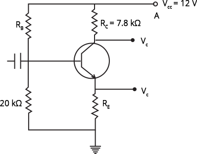
Ans: Let us reconstruct the given circuit,
${{I}_{C}}={{I}_{B}}+{{I}_{E}}$ …. because ${{I}_{B}}$ it is very small then ${{I}_{C}}$.
${{I}_{C}}={{I}_{E}}$
${{I}_{C}}=1mA$ …[Given]
${{I}_{E}}={{I}_{C}}={{10}^{-3}}A$
${{R}_{C}}=7.8k\Omega $
From the above-given figure,
${{I}_{C}}({{R}_{C}}+{{R}_{E}})+{{V}_{CE}}=12$
${{I}_{C}}({{R}_{C}}+{{R}_{E}})+1\times {{10}^{-3}}=12$
$({{R}_{C}}+{{R}_{E}})=\dfrac{9}{{{10}^{-3}}}$
$7.8\times {{10}^{3}}\times {{R}_{E}}=9000$
${{R}_{E}}=9000-7800=1200\Omega =1.2k\Omega $
Now, let's calculate VE
${{V}_{E}}={{I}_{C}}\times {{R}_{E}}={{I}_{C}}\times {{R}_{C}}=1200\times {{10}^{-3}}=1.2V$
${{V}_{B}}={{V}_{E}}+{{V}_{BE}}=1.2+0.5V=1.7V$
Finally, calculate current and the resistance,
$Current,I=\dfrac{{{V}_{B}}}{20000}=\dfrac{1.7}{20000}=0.085mA$
and, ${{R}_{B}}=\dfrac{{{V}_{B}}}{(I+{{I}_{B}})}$
${{R}_{B}}=\dfrac{12-1.7}{\dfrac{{{I}_{C}}}{\beta}+0.085}\times{{10}^{3}}=\dfrac{10.3}{0.01+0.085}=108k\Omega $
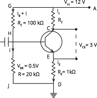
14.40 In the circuit shown in figure, find the value of Rc.
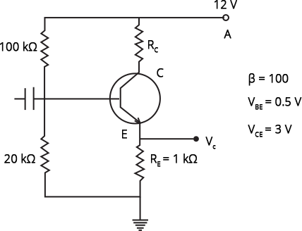
Ans: Given:
$\beta =100$
${{V}_{BE}}=0.5\text{ }V\text{ }$
${{V}_{CE}}=3\text{ }V$
Let's follow the circuit to solve the question,
${{I}_{E}}={{I}_{C}}+{{I}_{B}}\text{ }$
Also, ${{I}_{C}}=\beta {{I}_{B}}$
${{V}_{CC}}={{I}_{C}}{{R}_{C}}+{{V}_{CE}}+{{I}_{E}}{{R}_{E}}$
${{V}_{CC}}=R{{I}_{B}}+{{V}_{BE}}+{{I}_{E}}{{R}_{E}}$
${{I}_{E}}\approx {{I}_{C}}=\beta {{I}_{B}}$
Now,
${{V}_{CC}}-{{V}_{BE}}=R+(\beta {{R}_{E}}){{I}_{B}}$
${{I}_{B}}=\dfrac{{{V}_{CC}}-{{V}_{BE}}}{R+(\beta {{R}_{E}})}$
$=\dfrac{12-0.5}{80+1.2\times 100}=\dfrac{11.5}{200}mA$
Also,
$\left({{R}_{C}}+{{R}_{E}}\right)=\dfrac{{{V}_{CE}}-{{V}_{BE}}}{{{I}_{C}}}=\dfrac{{{V}_{CC}}-{{V}_{CE}}}{\beta{{I}_{B}}}$$\left({{R}_{C}}+{{R}_{E}}\right)=\dfrac{2}{11.5}\left(12-3\right)k\Omega =1.56k\Omega $ ${{R}_{C}}+{{R}_{E}}=1.56$
Therefore, ${{R}_{C}}=1.56-1=0.56k\Omega \text{ = 560}\Omega $
What is Semiconductor Electronics?
When Electrons mix with each other, due to closeness of atoms, it creates changes in the level of energy within the atoms. This leads to multiple bands of energy than a single energy level. The valence band has the highest amount of energy while the conduction band has the least amount. A forbidden energy gap is where Electrons cannot occupy any space. This is the space between the conduction and valence bands.
Semiconductors in particular carry levels of conductivity which lies between that of insulators and conductors. In Semiconductors, the forbidden energy gap is quite small. Silicon and germanium are two good examples of Semiconductors.
The NCERT Exemplar for Class 12 Physics, is a handy companion containing solutions solved by expert teachers at Vedantu as per the mandates of the CBSE’s NCERT textbook guidelines. Sign in to the website, register yourself and download the PDF!

FAQs on NCERT Exemplar for Class 12 Physics - Semiconductor Electronics - Free PDF Download
1. How can NCERT Exemplar help enhance my conceptual understanding?
The NCERT Textbooks cover Semiconductor Electronics adequately in their lucid presentation. Similarly, the NCERT Exemplar Class 12 Solutions lives up to its name, because it is prepared by subject experts as per the guidelines of the Central Board of Secondary Education (CBSE). It offers guided, step-by-step solutions to the NCERT exercises such as MCQs, short answer questions, long answer questions and so on. Thus, going through this document can help you get done with a complete revision of the Chapter. It will not just help you score more marks but strengthen your understanding of Semiconductor Electronics because of the way the solutions are prepared and structured.
2. What are some types of Semiconductors?
Intrinsic Semiconductors are also called pure Semiconductors because the Electrons equalling the number of holes are produced by thermal excitation. When an impure or dope material such as phosphorus is added to a pure Semiconductor through crystallization, it becomes an extrinsic or impure Semiconductor, capable of enhanced electrical conductivity. An N-type extrinsic Semiconductor is produced by adding little amounts of pentavalent impurities while a P-Type extrinsic Semiconductor is produced by adding little amounts of trivalent impurities.
3. What are the uses of Semiconductors?
As the title of the Chapter suggests, Semiconductors are primarily used to design Electronic components. They are used in diodes to allow current to flow in a single direction, thus creating a one-way electric valve. It is used in integrated chips in nanotechnology to enhance the functioning of Electronic components. Because Semiconductors also help produce light, they are used in LEDs, OLEDs, etc. Semiconductors are also used in solar technology, 3D printing machines, temperature sensors and even self-driving cars.
4. What are other useful resources I can use for Class 12 Physics ?
Class 12 Physics is a form of advanced Physics . It can be mind-boggling at times especially with the kind of theories and formulae it has. However, Vedantu as a platform which enables an effective format of personalized learning for thousands of students across India, offers multiple resources at your disposal for free! When you sign in and register to our website, you can find NCERT Exemplar and various other textbook solutions, Revision Notes and even CBSE Important Questions. These three serve different functions in your preparation. The NCERT Exemplar offers easy solutions to NCERT exercises, the Revision Notes offer a comprehensive view of the entire Chapter and the CBSE Important Questions are prepared based on questions from past year papers. Thus, you can prepare and score well as per your wish!
5. What are the topics covered in Class 12 Physics Chapter 14?
For those who wish to pursue engineering, especially Electronic or mechanical engineering as their future careers or wish to do anything related to Physics and Electronics - this is a fundamental Chapter that can help establish and enhance your basic understanding of this topic. Class 12 Physics Chapter 14 on Semiconductor Electronics covers major topics such as the Classification of metals, conductors and Semiconductors, extrinsic and intrinsic Semiconductors, Semiconductor diodes, p-n junction formation, special purpose p-n junction diodes, junction transistor, digital Electronics and logic gates.