


The cut- in voltage for silicon diode is approximately:
A) $0.2\,V$
B) $0.7\,V$
C) $1.1\,V$
D) $1.4\,V$
Answer
232.8k+ views
Hint: The silicon diode allows the accepting of the large electric current at a particular voltage called forward voltage. This is the cut- in voltage . Below this voltage, the diode does not allow the accepting of the current and after this the flow of current increases rapidly.
Complete step by step solution:
The silicon diode is made up of the silicon which has the two terminals in it. One of the terminal circuit elements minimizes the current flow in the one direction which is the reverse bias and in the other direction it carries the current easily which is known as the forward bias.
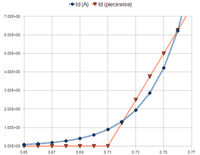
The $P$ type of the silicon diode possesses one extra hole in it. The battery in this diode is connected across the $p - n$ junction which makes the diode as the forward biased. Hence it pushes the electrons moves from the $n$ type to that of the $p$ type whereas the holes moves from the $p$ type to that of the $n$ type. This silicon diode requires $0.7\,V$ to start the forward biasing and this is known as the cut in voltage.
Thus the option (B) is correct.
Note: The semiconductors like germanium and the silicon are mainly used for the purpose of the diode. The germanium diode is more advantageous when compared to that of the silicon diode. Since the germanium diode requires only $0.3\,V$ to start forward biasing the diode. And the schottky requires only $0.2\,V$ for forward biasing.
Complete step by step solution:
The silicon diode is made up of the silicon which has the two terminals in it. One of the terminal circuit elements minimizes the current flow in the one direction which is the reverse bias and in the other direction it carries the current easily which is known as the forward bias.
The $P$ type of the silicon diode possesses one extra hole in it. The battery in this diode is connected across the $p - n$ junction which makes the diode as the forward biased. Hence it pushes the electrons moves from the $n$ type to that of the $p$ type whereas the holes moves from the $p$ type to that of the $n$ type. This silicon diode requires $0.7\,V$ to start the forward biasing and this is known as the cut in voltage.
Thus the option (B) is correct.
Note: The semiconductors like germanium and the silicon are mainly used for the purpose of the diode. The germanium diode is more advantageous when compared to that of the silicon diode. Since the germanium diode requires only $0.3\,V$ to start forward biasing the diode. And the schottky requires only $0.2\,V$ for forward biasing.
Recently Updated Pages
Circuit Switching vs Packet Switching: Key Differences Explained
JEE General Topics in Chemistry Important Concepts and Tips
JEE Extractive Metallurgy Important Concepts and Tips for Exam Preparation
JEE Amino Acids and Peptides Important Concepts and Tips for Exam Preparation
JEE Atomic Structure and Chemical Bonding important Concepts and Tips
Electricity and Magnetism Explained: Key Concepts & Applications
Trending doubts
JEE Main 2026: Session 2 Registration Open, City Intimation Slip, Exam Dates, Syllabus & Eligibility
JEE Main 2026 Application Login: Direct Link, Registration, Form Fill, and Steps
JEE Main Marking Scheme 2026- Paper-Wise Marks Distribution and Negative Marking Details
Understanding the Angle of Deviation in a Prism
Hybridisation in Chemistry – Concept, Types & Applications
How to Convert a Galvanometer into an Ammeter or Voltmeter
Other Pages
JEE Advanced Marks vs Ranks 2025: Understanding Category-wise Qualifying Marks and Previous Year Cut-offs
Dual Nature of Radiation and Matter Class 12 Physics Chapter 11 CBSE Notes - 2025-26
Understanding Uniform Acceleration in Physics
Understanding the Electric Field of a Uniformly Charged Ring
JEE Advanced Weightage 2025 Chapter-Wise for Physics, Maths and Chemistry
Derivation of Equation of Trajectory Explained for Students