


The valence of an impurity added to germanium crystal in order to convert it into a P− type semiconductor is
A. 6
B. 5
C. 4
D. 3
Answer
252.9k+ views
Hint:Trivalent impurity atom i.e., atoms having 3 valence electrons, when added to a pure semiconductor, produce additional free electrons which are donor electrons to the semiconductor.
Complete step by step solution:
1.Doping is the addition of impurities to intrinsic semiconductors in order to change their characteristics.
2.To dope silicon and germanium, typically trivalent and pentavalent elements are utilised.
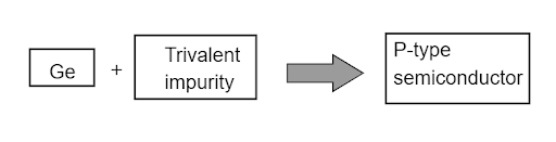
3. When a trivalent impurity is used to dope an intrinsic semiconductor, the result is a P-Type semiconductor.
4.A p-type semiconductor results from implanting a dopant atom.
5.The answer is option D -3 valence electrons.
Hence, the correct option is D.
Additional information: A semiconductor material has electrical conductivity that is in the range of an insulator like glass and a conductor like metallic copper. As the temperature increases, its resistivity decreases; metals respond in the reverse way.
Diodes, transistors, and integrated circuits are just a few of the different types of electronic devices that are made using semiconductors.
Properties of semiconductor:
1. A semiconductor has a higher resistivity than a conductor but a lower resistance than an insulator.
2. The temperature coefficient of resistance for semiconductors is negative. In layman's terms, semiconductor resistance lowers as temperature rises and vice versa.
3. Semiconductors act as insulators when the temperature is 0 kelvin. It functions as a conductor when the temperature rises.
4. When impurities are added, the conductivity of the semiconductors rises. Doping is the process of introducing impurities into semiconductors.
Note: An inherent semiconductor doped with boron (B) or indium is known as a p-type semiconductor. Boron from Group III has three valence electrons, while silicon from Group IV has four.
Complete step by step solution:
1.Doping is the addition of impurities to intrinsic semiconductors in order to change their characteristics.
2.To dope silicon and germanium, typically trivalent and pentavalent elements are utilised.
3. When a trivalent impurity is used to dope an intrinsic semiconductor, the result is a P-Type semiconductor.
4.A p-type semiconductor results from implanting a dopant atom.
5.The answer is option D -3 valence electrons.
Hence, the correct option is D.
Additional information: A semiconductor material has electrical conductivity that is in the range of an insulator like glass and a conductor like metallic copper. As the temperature increases, its resistivity decreases; metals respond in the reverse way.
Diodes, transistors, and integrated circuits are just a few of the different types of electronic devices that are made using semiconductors.
Properties of semiconductor:
1. A semiconductor has a higher resistivity than a conductor but a lower resistance than an insulator.
2. The temperature coefficient of resistance for semiconductors is negative. In layman's terms, semiconductor resistance lowers as temperature rises and vice versa.
3. Semiconductors act as insulators when the temperature is 0 kelvin. It functions as a conductor when the temperature rises.
4. When impurities are added, the conductivity of the semiconductors rises. Doping is the process of introducing impurities into semiconductors.
Note: An inherent semiconductor doped with boron (B) or indium is known as a p-type semiconductor. Boron from Group III has three valence electrons, while silicon from Group IV has four.
Recently Updated Pages
States of Matter Chapter For JEE Main Chemistry
Young’s Double Slit Experiment Derivation Explained
JEE Main Participating Colleges 2026 - A Complete List of Top Colleges
Wheatstone Bridge – Principle, Formula, Diagram & Applications
Circuit Switching vs Packet Switching: Key Differences Explained
Mass vs Weight: Key Differences Explained for Students
Trending doubts
JEE Main 2026: Exam Dates, Session 2 Updates, City Slip, Admit Card & Latest News
JEE Main Marking Scheme 2026- Paper-Wise Marks Distribution and Negative Marking Details
JEE Main 2026 Application Login: Direct Link, Registration, Form Fill, and Steps
Hybridisation in Chemistry – Concept, Types & Applications
Understanding the Electric Field of a Uniformly Charged Ring
Derivation of Equation of Trajectory Explained for Students
Other Pages
CBSE Class 12 Physics Question Paper 2026: Download SET-wise PDF with Answer Key & Analysis
JEE Advanced 2026 - Exam Date (Released), Syllabus, Registration, Eligibility, Preparation, and More
JEE Advanced Marks vs Ranks 2025: Understanding Category-wise Qualifying Marks and Previous Year Cut-offs
JEE Advanced Weightage 2025 Chapter-Wise for Physics, Maths and Chemistry
Ideal and Non-Ideal Solutions Explained for Class 12 Chemistry
JEE Advanced Marks vs Rank 2025 - Predict Your IIT Rank Based on Score