


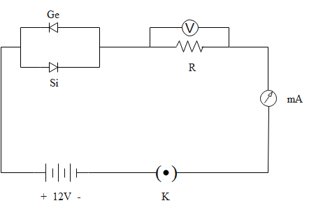
Germanium and silicon junction diodes are connected in parallel. These are connected in series with a resistance $\mathrm{R}$, a milliammeter $(\mathrm{mA})$ and a key $(\mathrm{K})$ as shown in Fig. When key $(\mathbf{K})$ is closed a current begins to flow in the milliammeter. The potential drop across the germanium diode is then
(A) 0.3 V
(B) 0.7 V
(C) 1.1 V
(D) 12 V
Answer
249.6k+ views
Hint: We know that diode (PN junction) in an electrical circuit allows current to flow more easily in one direction than another. Forward biasing means putting a voltage across a diode that allows current to flow easily, while reverse biasing means putting a voltage across a diode in the opposite direction. The Forward bias decreases the resistance of the diode whereas the reversed bias increases the resistance of the diode. In forward biasing the current is easily flowing through the circuit whereas reverse bias does not allow the current to flow through it.
Complete step by step answer
We know that forward bias or biasing is where the external voltage is delivered across the P-N junction diode. In a forward bias setup, the P-side of the diode is attached to the positive terminal and N-side is fixed to the negative side of the battery.
Reverse biased diode means that the positive end of the battery is connected to the negative end of the diode and the negative end of the battery is connected to the positive end of the diode. A diode is an electrical component acting as a one-way valve for current. When voltage is applied across a diode in such a way that the diode allows current, the diode is said to be forward-biased.
The germanium diode is reverse biased and the silicon diode is forward biased. Therefore, there will be no current in the branch of germanium diode. The potential barrier of silicon diode is $0.7 \mathrm{V}$. Therefore, for conduction minimum potential difference across silicon is $0.7 \mathrm{V}$.
Maximum potential difference across resistance, $\mathrm{R}=12-0.7=$$11.3 \mathrm{V}$
So, the correct answer is option B.
Note: The forward bias causes a force on the electrons pushing them from the N side toward the P side. With forward bias, the depletion region is narrow enough that electrons can cross the junction and inject into the p-type material. The width of the depletion layer in a p-n junction diode decreases in forward bias due to repulsion of carriers from battery terminals, holes from p-type and electrons from n-type. Now, due to the small number of ions in the depletion region its potential decreases. Due to this increased depletion width and barrier potential, no charge carriers have the energy to cross the junction so no current flows across the diode. If two diodes are connected in parallel, both forward biased, then current flows through the diode having lesser barrier potential.
Recently Updated Pages
JEE Isolation, Preparation and Properties of Non-metals Important Concepts and Tips for Exam Preparation
Isoelectronic Definition in Chemistry: Meaning, Examples & Trends
Ionisation Energy and Ionisation Potential Explained
Iodoform Reactions - Important Concepts and Tips for JEE
Introduction to Dimensions: Understanding the Basics
Instantaneous Velocity Explained: Formula, Examples & Graphs
Trending doubts
JEE Main 2026: Exam Dates, Session 2 Updates, City Slip, Admit Card & Latest News
Hybridisation in Chemistry – Concept, Types & Applications
JEE Main 2026 Application Login: Direct Link, Registration, Form Fill, and Steps
Understanding the Electric Field of a Uniformly Charged Ring
Derivation of Equation of Trajectory Explained for Students
JEE Main Marking Scheme 2026- Paper-Wise Marks Distribution and Negative Marking Details
Other Pages
CBSE Class 12 Physics Question Paper 2026: Download SET-wise PDF with Answer Key & Analysis
JEE Advanced Marks vs Ranks 2025: Understanding Category-wise Qualifying Marks and Previous Year Cut-offs
JEE Advanced 2026 - Exam Date (Released), Syllabus, Registration, Eligibility, Preparation, and More
JEE Advanced Weightage 2025 Chapter-Wise for Physics, Maths and Chemistry
Understanding the Angle of Deviation in a Prism
Understanding Centrifugal Force in Physics