


For the given logic diagram, output \[F = 1\] , then inputs are:
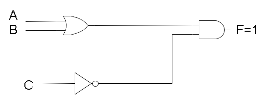
A) \[A = 0,B = 0,C = 0\]
B) \[A = 0,B = 1,C = 0\]
C) \[A = 1,B = 1,C = 1\]
D) \[A = 0,B = 0,C = 1\]
Answer
261k+ views
Hint: In this solution, we will find the logic equation for the output of F. A and B terminals are connected to an OR gate while C is connected to a NOT gate.
Complete step by step answer:
As given in the image, we can see that A and B are connected to an OR gate.
This gives an output of $A + B$
The C terminal is connected to a NOT gate which gives us output $\bar C$
Both these gates are then connected by an AND gate so the net output would be
$F = \left( {A + B} \right).\bar C$
For the output F to be 1, we can see that both of the inputs of the final and gate must be one. Hence for the input coming from the C terminal to be 1, the input of C must be zero i.e. $C = 0.$
For the input coming from the A or B gate, either A or B must be one. From the options, we can see that the only option satisfying the above conditions is option (B).
The configuration \[A = 0,B = 1,C = 0\] will give an output of 1 in the following way. The combination of A OR B will give a 1 since $B = 1$. The output of $\bar C$ will be 1 since the input of C is zero.
Hence the combination of both inputs of the AND gate is 1 so the final output will also be 1.
Hence the correct choice is option (B).
Note: In such questions, it is helpful to check all the options one by one to determine which set of inputs will give the output of 1. So we must be aware of the output table of different kinds of logic gates to answer this question.
Recently Updated Pages
Algebra Made Easy: Step-by-Step Guide for Students
JEE Isolation, Preparation and Properties of Non-metals Important Concepts and Tips for Exam Preparation
JEE Energetics Important Concepts and Tips for Exam Preparation
Chemical Properties of Hydrogen - Important Concepts for JEE Exam Preparation
JEE General Topics in Chemistry Important Concepts and Tips
JEE Amino Acids and Peptides Important Concepts and Tips for Exam Preparation
Trending doubts
JEE Main 2026: Exam Dates, Session 2 Updates, City Slip, Admit Card & Latest News
JEE Main Participating Colleges 2026 - A Complete List of Top Colleges
Hybridisation in Chemistry – Concept, Types & Applications
Understanding the Electric Field of a Uniformly Charged Ring
Derivation of Equation of Trajectory Explained for Students
Understanding Atomic Structure for Beginners
Other Pages
CBSE Class 12 Physics Question Paper 2026: Download SET-wise PDF with Answer Key & Analysis
JEE Advanced 2026 Notification Out with Exam Date, Registration (Extended), Syllabus and More
JEE Advanced Marks vs Ranks 2025: Understanding Category-wise Qualifying Marks and Previous Year Cut-offs
JEE Advanced Weightage Chapter Wise 2026 for Physics, Chemistry, and Mathematics
How to Convert a Galvanometer into an Ammeter or Voltmeter
Understanding Uniform Acceleration in Physics