


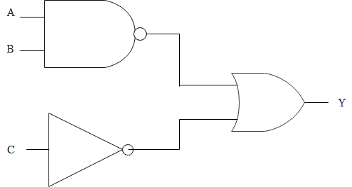
The input to the digital circuit are as shown below: The output Y is:
(A) $A+B+\bar{C}$
(B) $(A+B) \bar{C}$
(C) $\bar{A}+\bar{B}+\bar{C}$
(D) $\bar{A}+\bar{B}+C$
Answer
253.8k+ views
Hint: We know that a Digital Logic Gate is an electronic circuit which makes logical decisions based on the combination of digital signals present on its inputs. Digital logic gates can have more than one input, for example, inputs A, B, C, D etc., but generally only have one digital output, (Q). Digital logic is fundamental in creating electronic devices. It is used to create circuits and logic gates, as well as to check computer chips. Knowledge of digital logic lends itself to many different computer technology design and engineering professions.
Complete step by step answer
We know that logic gates perform basic logical functions and are the fundamental building blocks of digital integrated circuits. Most logic gates take an input of two binary values, and output a single value of a 1 or 0. Some circuits may have only a few logic gates, while others, such as microprocessors, may have millions of them.
We can say that NAND and NOR can be used to build any of the gates i.e. AND, OR, NOT, XOR, XNOR. That is why all the gates are made using these two gates only. not only it reduces cost for building different gates over a chip, it reduces the hardware also. NAND and NOR are preferred because they are smaller and use less power in a CMOS process than equivalent AND or OR gates. NAND and NOR gates can be created with 4 transistors, while AND/OR require 6. An AND/OR gate is laid out in a cell library generally as a NAND/NOR followed by an inverter.
We can say that:
$\mathrm{A}$ and $\mathrm{B}$ are inputs to the NAND gate. The output of that gate is $\overline{(\mathrm{A.B})}=\overline{\mathrm{A}}+\overline{\mathrm{B}}$
The output of $\mathrm{C}$ being input to the NOT gate is $\overline{\mathrm{C}}$. These two are inputs of the OR gate. Hence $\mathrm{Y}=\overline{(\mathrm{A.B})}+\overline{\mathrm{C}}$
$=\overline{\mathrm{A}}+\overline{\mathrm{B}}+\overline{\mathrm{C}}$
Hence the correct answer is option C.
Note: We know that the AND gate is so named because, if 0 is called "false" and 1 is called "true," the gate acts in the same way as the logical "and" operator. The output is "true" when both inputs are "true." Otherwise, the output is "false." In other words, the output is 1 only when both inputs one AND two are 1. When a transistor is on, or open, then an electric current can flow through. When we string a bunch of these transistors together, then we get what's called a logic gate, which lets us add, subtract, multiply, and divide binary numbers in any way imaginable. In a physical circuit, these logic gates have: Inputs.
Recently Updated Pages
States of Matter Chapter For JEE Main Chemistry
Young’s Double Slit Experiment Derivation Explained
JEE Main Participating Colleges 2026 - A Complete List of Top Colleges
Wheatstone Bridge – Principle, Formula, Diagram & Applications
Circuit Switching vs Packet Switching: Key Differences Explained
Mass vs Weight: Key Differences Explained for Students
Trending doubts
JEE Main 2026: Exam Dates, Session 2 Updates, City Slip, Admit Card & Latest News
JEE Main Marking Scheme 2026- Paper-Wise Marks Distribution and Negative Marking Details
JEE Main 2026 Application Login: Direct Link, Registration, Form Fill, and Steps
Hybridisation in Chemistry – Concept, Types & Applications
Understanding the Electric Field of a Uniformly Charged Ring
Derivation of Equation of Trajectory Explained for Students
Other Pages
CBSE Class 12 Physics Question Paper 2026: Download SET-wise PDF with Answer Key & Analysis
JEE Advanced 2026 - Exam Date (Released), Syllabus, Registration, Eligibility, Preparation, and More
JEE Advanced Marks vs Ranks 2025: Understanding Category-wise Qualifying Marks and Previous Year Cut-offs
JEE Advanced Weightage 2025 Chapter-Wise for Physics, Maths and Chemistry
Ideal and Non-Ideal Solutions Explained for Class 12 Chemistry
JEE Advanced Marks vs Rank 2025 - Predict Your IIT Rank Based on Score