


The forward biased diode connection is:
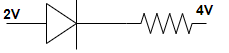
(A)
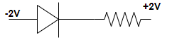
(B)
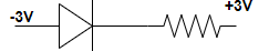
(C)

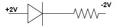
(D)
Answer
232.8k+ views
Hint: This question can be solved by having an understanding of a semiconductor device that is known as p-n junction or junction diode. These kinds of devices are made of semiconductor materials having the energy band gap of \[ < 3\]eV between conduction band and valence band.
Complete step by step answer:
Step 1: A p-n junction or junction diode is said to be in forward bias if the positive terminal of the external battery B is connected to the p-side and the negative terminal is connected to the n-side of p-n junction.
The majority carriers, electrons in the n-region are repelled by the negative potential due to battery B and move towards the p-n junction. Similarly, the majority carriers, holes in the p-region are repelled by the positive potential due to battery B, towards the junction.
The positive potential of p-region attracts the electrons from the n-region and negative potential of n-region attracts the holes from the p-region.
Step 2: As shown in this question from all the given options, option (C) is in forward bias in which the p-side of the diode is connected to the +2V of the battery and n-side of the diode is connected to the -2V of the battery.
As we know that majority carriers, holes in the p-region will be repelled and majority carriers, electrons in the n-region will be repelled. Due to this, the diffusion of majority carriers takes place across the junction.
So, this given configuration is in forward bias i.e. the option (C) is correct.
Note: It should always be remembered that at zero kelvin temperature, electrons are not able to cross even the given energy band gap and hence the conduction band remains totally empty. Therefore, the semiconductor at zero kelvin behaves as an insulator.
Recently Updated Pages
JEE Main 2026 Session 2 Registration Open, Exam Dates, Syllabus & Eligibility
JEE Main 2023 April 6 Shift 1 Question Paper with Answer Key
JEE Main 2023 April 6 Shift 2 Question Paper with Answer Key
JEE Main 2023 (January 31 Evening Shift) Question Paper with Solutions [PDF]
JEE Main 2023 January 30 Shift 2 Question Paper with Answer Key
JEE Main 2023 January 25 Shift 1 Question Paper with Answer Key
Trending doubts
JEE Main Marking Scheme 2026- Paper-Wise Marks Distribution and Negative Marking Details
Why does capacitor block DC and allow AC class 12 physics JEE_Main
Understanding Average and RMS Value in Electrical Circuits
Understanding Collisions: Types and Examples for Students
Ideal and Non-Ideal Solutions Explained for Class 12 Chemistry
Understanding Atomic Structure for Beginners
Other Pages
JEE Advanced Weightage 2025 Chapter-Wise for Physics, Maths and Chemistry
CBSE Class 12 Physics Set 2 (55/2/2) 2025 Question Paper & Solutions
Inductive Effect and Its Role in Acidic Strength
Degree of Dissociation: Meaning, Formula, Calculation & Uses
Units and Measurements Mock Test for JEE Main 2025-26 Preparation
Chemistry Question Papers for JEE Main, NEET & Boards (PDFs)