


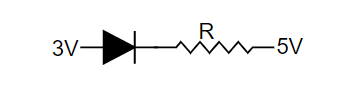
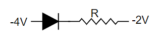
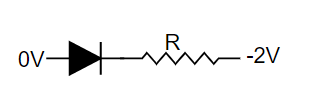
Which of the following represents a forward bias diode?
$\left( a \right)$
$\left( b \right)$

$\left( c \right)$
$\left( d \right)$

Answer
243.3k+ views
Hint: This type of question is based on the concept of the diode. As we know that the in forward bias, a p-type semiconductor is at a higher potential as compared to an n-type semiconductor. So by using this concept we will be able to answer this question.
Complete Step By Step Solution: In forward bias, the $p$ side of $p - n$ the junction is connected to higher potential, and $n$ the side of $p - n$ the junction is connected to lower potential. So we can say that the potential will be higher than another side.
Now we will look into the figure,
As we can see in the option $\left( b \right)$ the potential on the left side is much higher than the potential on the right side. So we can say that this diode represents the forward bias diode.
Therefore, the option $\left( b \right)$ is correct.
Additional information: Forward bias in the electronics world is when, in a SEMICONDUCTOR device, when we connect its $P - type$ , positive doped region, i.e. with B, Al, etc. to the positive terminal of the battery and $N - type$ , Negative doped I.e. with N, P, etc. to the negative terminal of the battery.
Forward bias, the immediate current-voltage is needed to keep up the current stream in a bipolar semiconductor or diode or to improve the current stream in a field-impact semiconductor. A silicon diode will lead current just if its anode is at a positive voltage contrasted with its cathode; it is then supposed to be forward one-sided.
Note: As we can see that this question becomes very easy when we know about the properties or we can say the definition of it. So we should have to understand the concept and memorize the properties of bias to answer the question.
Recently Updated Pages
JEE Main 2026 Session 2 City Intimation Slip & Exam Date: Expected Date, Download Link
JEE Main 2026 Session 2 Application Form: Reopened Registration, Dates & Fees
JEE Main 2026 Session 2 Registration (Reopened): Last Date, Fees, Link & Process
WBJEE 2026 Registration Started: Important Dates Eligibility Syllabus Exam Pattern
JEE Main 2025-26 Mock Tests: Free Practice Papers & Solutions
JEE Main 2025-26 Experimental Skills Mock Test – Free Practice
Trending doubts
JEE Main 2026: Exam Dates, Session 2 Updates, City Slip, Admit Card & Latest News
Ideal and Non-Ideal Solutions Explained for Class 12 Chemistry
Understanding the Angle of Deviation in a Prism
Understanding Differential Equations: A Complete Guide
Hybridisation in Chemistry – Concept, Types & Applications
Understanding the Electric Field of a Uniformly Charged Ring
Other Pages
CBSE Class 12 Physics Question Paper 2026: Download SET-wise PDF with Answer Key & Analysis
JEE Advanced Marks vs Ranks 2025: Understanding Category-wise Qualifying Marks and Previous Year Cut-offs
JEE Advanced 2026 - Exam Date (Released), Syllabus, Registration, Eligibility, Preparation, and More
Dual Nature of Radiation and Matter Class 12 Physics Chapter 11 CBSE Notes - 2025-26
JEE Advanced Weightage 2025 Chapter-Wise for Physics, Maths and Chemistry
Understanding the Block and Tackle System