


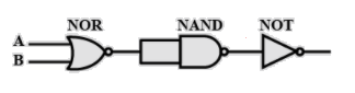
The equivalent circuit is:
(A) NAND gate
(B) OR gates
(C) AND gates
(D) NOR gates
Answer
257.4k+ views
Hint: From the question we know that the circuit has a NOR gate, NAND gate, and a NOT gate. The input is sent to the NOR gate and the output of that becomes the input for NAND and the output of the NAND gate becomes the input for NOT gate. What exactly happens in each of these gates,
(1) In a NOR gate, the output is the inverse of the sum of A and B. (NOR, $OUTPUT = \overline {A + B} $).
(2) In a NAND gate, the output is the inverse of the multiplication of A and B. (NAND, $OUTPUT = \overline {A.B} $).
(3) in a NOT gate the output is the inverse of the input, the input of a NOT gate is always a single digit. ( NOT,$OUTPUT = \overline A $).
Complete step by step solution:
Taking outputs of all the gates as ${y_1},{y_2},{y_3}$,
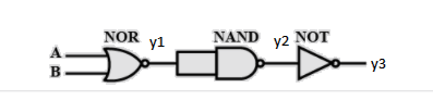
We know that a NOR gate inverses the sum of its inputs , so output at NOR is ${y_1} = \overline {A + B} $
${y_1}$ becomes the input for NAND gate , so $\overline {{y_1}.{y_1}} = {y_2} = \overline {\overline {A + B} .\overline {A + B} } = \overline {\overline {A + B} } + \overline {\overline {A + B} } = A + B$
${y_2}$ become the input for NOT gate , so, ${y_3} = \overline {{y_2}} = \overline {A + B} $
The output for the NOT gate is ${y_3}$ which is the final output and we get the output as the inverse of the sum of A and B which is nothing but the output of NOR gate.
Here, ${y_1},{y_2},{y_3}$ are the outputs of NOR, NAND and NOT gates respectively . The final output is ${y_3}$.
Hence option (D), NOR gate is the correct answer.
Note: Do not get confused with the diagram as OR and AND and NOT the small circle beside each of the gates makes them NOR and NAND gates. It represents the negation of OR and AND. The N represents “negation of” which means the inverse.
(1) In a NOR gate, the output is the inverse of the sum of A and B. (NOR, $OUTPUT = \overline {A + B} $).
(2) In a NAND gate, the output is the inverse of the multiplication of A and B. (NAND, $OUTPUT = \overline {A.B} $).
(3) in a NOT gate the output is the inverse of the input, the input of a NOT gate is always a single digit. ( NOT,$OUTPUT = \overline A $).
Complete step by step solution:
Taking outputs of all the gates as ${y_1},{y_2},{y_3}$,
We know that a NOR gate inverses the sum of its inputs , so output at NOR is ${y_1} = \overline {A + B} $
${y_1}$ becomes the input for NAND gate , so $\overline {{y_1}.{y_1}} = {y_2} = \overline {\overline {A + B} .\overline {A + B} } = \overline {\overline {A + B} } + \overline {\overline {A + B} } = A + B$
${y_2}$ become the input for NOT gate , so, ${y_3} = \overline {{y_2}} = \overline {A + B} $
The output for the NOT gate is ${y_3}$ which is the final output and we get the output as the inverse of the sum of A and B which is nothing but the output of NOR gate.
Here, ${y_1},{y_2},{y_3}$ are the outputs of NOR, NAND and NOT gates respectively . The final output is ${y_3}$.
Hence option (D), NOR gate is the correct answer.
Note: Do not get confused with the diagram as OR and AND and NOT the small circle beside each of the gates makes them NOR and NAND gates. It represents the negation of OR and AND. The N represents “negation of” which means the inverse.
Recently Updated Pages
JEE Main Mock Test 2025-26: Electromagnetic Induction & Alternating Currents
JEE Main Mock Test 2025-26: Optics Chapter Practice Online
JEE Main 2025-26 Mock Test: Properties of Solids and Liquids
JEE Main Mock Test 2025-26: Dual Nature of Matter & Radiation
JEE Main 2025-26 Electromagnetic Waves Mock Test with Solutions
JEE Main 2025-26 Mock Test: Electronic Devices Chapter Practice
Trending doubts
JEE Main 2026: Exam Dates, Session 2 Updates, City Slip, Admit Card & Latest News
JEE Main Participating Colleges 2026 - A Complete List of Top Colleges
JEE Main 2026 Application Login: Direct Link, Registration, Form Fill, and Steps
JEE Main Colleges 2026: Complete List of Participating Institutes
JEE Main Marking Scheme 2026- Paper-Wise Marks Distribution and Negative Marking Details
Hybridisation in Chemistry – Concept, Types & Applications
Other Pages
CBSE Class 12 Physics Question Paper 2026: Download SET-wise PDF with Answer Key & Analysis
JEE Advanced 2026 - Exam Date (Released), Syllabus, Registration, Eligibility, Preparation, and More
JEE Advanced Marks vs Ranks 2025: Understanding Category-wise Qualifying Marks and Previous Year Cut-offs
JEE Advanced Weightage 2025 Chapter-Wise for Physics, Maths and Chemistry
Understanding the Electric Field of a Uniformly Charged Ring
Derivation of Equation of Trajectory Explained for Students