


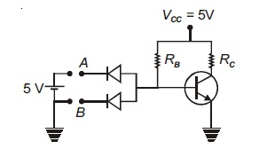
Figure shows practical realization of logic gates. Identify the logic gate
(A) NAND
(B) NOR
(C) XOR
(D) XNOR
Answer
264.3k+ views
Hint: We can assume the possible cases for point A and B, observe the output of the transistor for each case then match it with the truth table of the gates of NAND, NOR, XOR and XNOR options to get the answer.
Complete step by step answer:
As shown in the figure, point A and B can be at 0 (level 0) or 5V (level 1) with the help of battery.
There are four possible cases- when both A and B are earthed, when A is connected and B is earthed, when B is connected and A is earthed, when both A and B are connected to the battery.
Let us take a possibility - when A is connected to the positive terminal of the battery and B is earthed (A=1 and B=0) then the upper diode is reversed biased and the lower one is forward biased. Due to voltage difference the base current will flow. Hence current will flow in the collector region of the transistor and we will get an output as 1.
When both A and B are connected then diodes are off hence at the end of base resistance the potential will be zero. Hence, the transistor will be saturated, and the output will be 0.
If we check for the remaining two possibilities, we see that the truth table obtained is that of NAND gate.
Hence, the correct option is A. NAND
Note:
On observing carefully, we can see that NAND is nothing but the complement of AND gate. NAND is also known as a universal gate along with NOR as both these logic gates can be used to produce different gates.
Recently Updated Pages
JEE Main 2025-26 Experimental Skills Mock Test – Free Practice
JEE Main 2025-26 Electronic Devices Mock Test: Free Practice Online
JEE Main 2025-26 Mock Tests: Free Practice Papers & Solutions
JEE Main 2025-26: Magnetic Effects of Current & Magnetism Mock Test
JEE Main 2025-26 Atoms and Nuclei Mock Test – Free Practice Online
JEE Main Mock Test 2025-26: Experimental Skills Chapter Online Practice
Trending doubts
JEE Main 2026: Exam Dates, Session 2 Updates, City Slip, Admit Card & Latest News
JEE Main Participating Colleges 2026 - A Complete List of Top Colleges
Kinematics Mock Test for JEE Main 2025-26: Comprehensive Practice
Kinematics Mock Test for JEE Main 2025-26: Practice & Ace the Exam
Hybridisation in Chemistry – Concept, Types & Applications
Understanding the Electric Field of a Uniformly Charged Ring
Other Pages
CBSE Class 12 Physics Question Paper 2026: Download SET-wise PDF with Answer Key & Analysis
JEE Advanced 2026 Notification Out with Exam Date, Registration (Extended), Syllabus and More
JEE Advanced Percentile vs Marks 2026: JEE Main Cutoff, AIR & IIT Admission Guide
JEE Advanced Weightage Chapter Wise 2026 for Physics, Chemistry, and Mathematics
JEE Advanced Marks vs Rank 2025 - Predict Your IIT Rank Based on Score
Derivation of Equation of Trajectory Explained for Students