


What Are the Main Types and Functions of Electronic Devices?
Electronic devices are fundamental components in modern physics and engineering, serving as the basis for understanding semiconductor behavior and circuit design. This topic covers the structure, functioning, and applications of various electronic devices, which are important for JEE Main Physics exam preparation.
Energy Bands in Solids
Solids have discrete energy levels that form continuous bands due to atomic interactions. The two primary bands are the valence band and the conduction band, separated by a forbidden energy gap.
The valence band consists of electrons bound to atoms, while the conduction band contains free electrons contributing to electrical conductivity.
Classification of Materials
Materials are classified as conductors, insulators, or semiconductors based on the size of the forbidden energy gap between their valence and conduction bands.
- Conductors: Very small or zero energy gap
- Insulators: Large energy gap, minimal conduction
- Semiconductors: Intermediate energy gap
Semiconductors: Types and Doping
Semiconductors can be intrinsic or extrinsic. Intrinsic semiconductors are pure elements like germanium (Ge) and silicon (Si). Extrinsic semiconductors are formed by doping intrinsic semiconductors with impurities to improve conductivity.
Doping with pentavalent impurities (donors) forms n-type semiconductors with electrons as majority charge carriers. Doping with trivalent impurities (acceptors) forms p-type semiconductors where holes are majority charge carriers.
Properties and Equations in Semiconductors
The product of the concentrations of free electrons ($n_e$) and holes ($n_h$) in a semiconductor at thermal equilibrium is a constant for a given temperature, given by the mass action law:
${n_e} \times {n_h} = {n_i}^2$
The electrical conductivity of intrinsic and extrinsic semiconductors is described by:
Intrinsic: $\sigma = e (n_e \mu_e + n_h \mu_h)$
Extrinsic (n-type): $\sigma = e n_e \mu_e$; (p-type): $\sigma = e n_h \mu_h$
PN-Junction Diode
A PN-junction diode is a two-terminal electronic device formed by joining p-type and n-type semiconductors. The junction shows different current conduction behavior based on the applied voltage polarity.
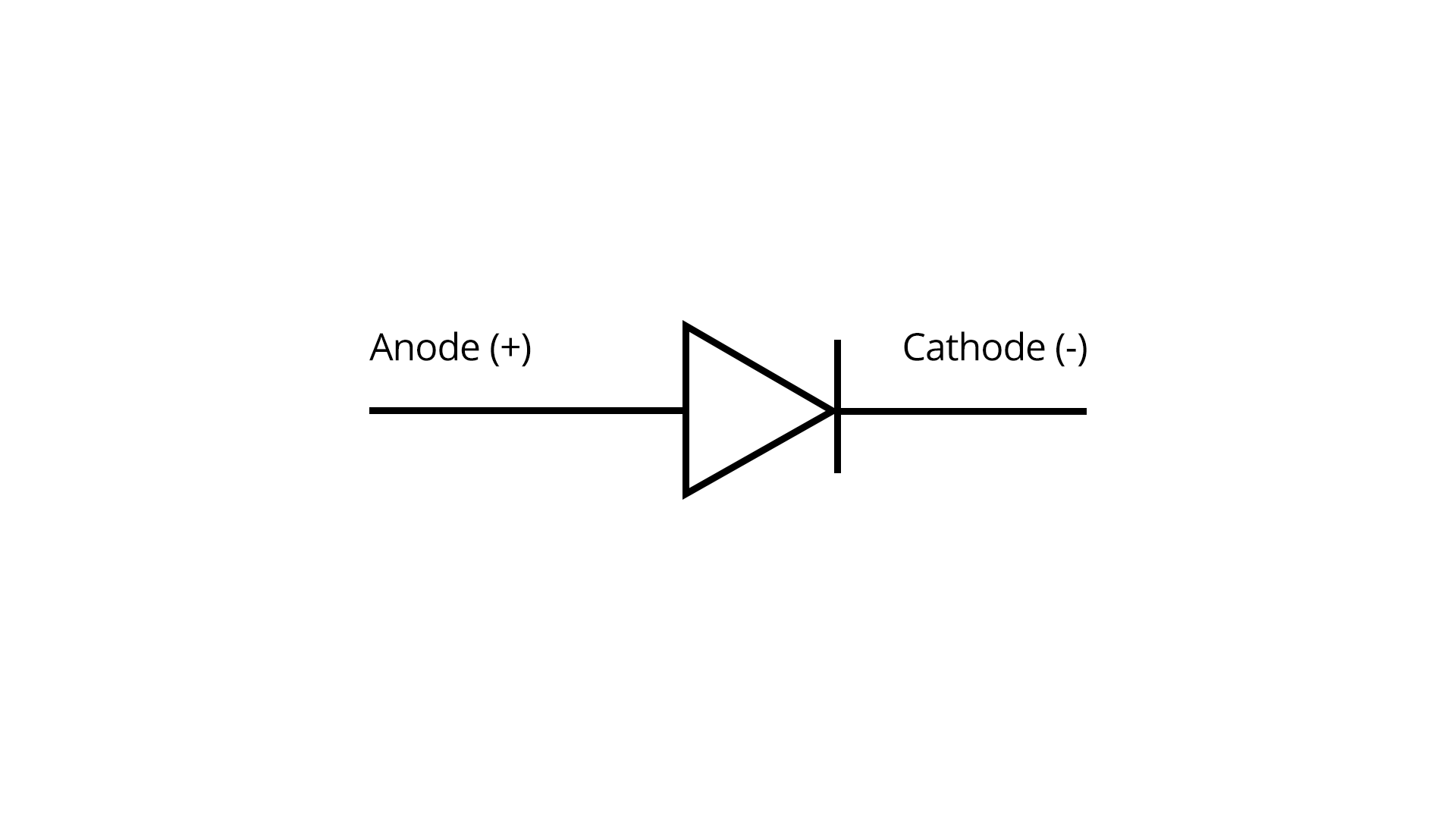
In forward bias, the p-side is connected to the positive terminal and the n-side to the negative terminal, allowing current to flow. In reverse bias, the current is blocked except for a small leakage current.
The diode current in forward bias is given by Shockley's equation:
$I = I_0 \left(e^{\dfrac{qV}{kT}} - 1\right)$
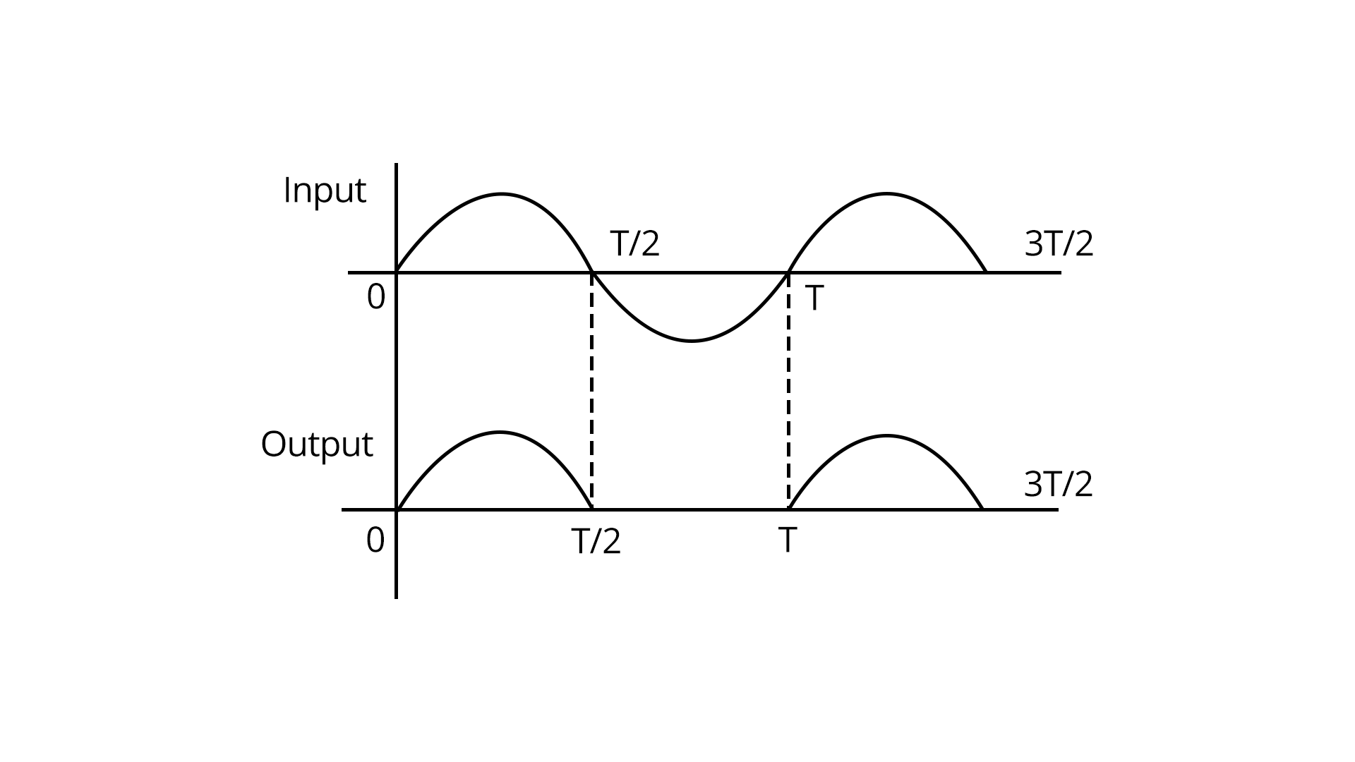
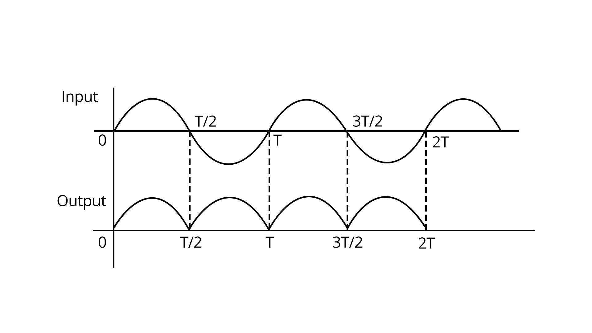
Rectifiers and Their Types
Rectifiers are circuits that convert alternating current (AC) into direct current (DC) using diodes. There are two main types: half-wave and full-wave rectifiers.
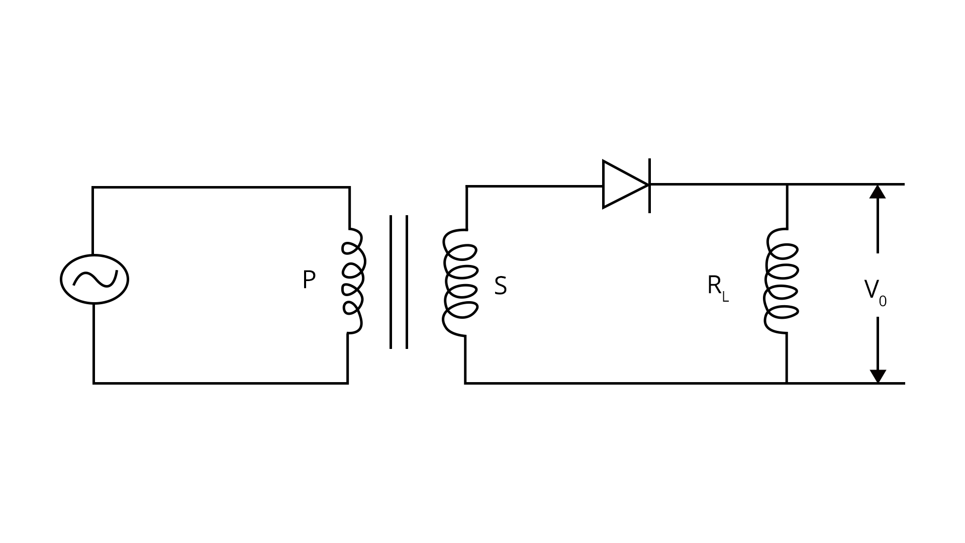
Half-wave rectifiers allow current during only one half of the input AC cycle, whereas full-wave rectifiers conduct for both halves.
The form factor and ripple factor are important parameters for rectifier design and analysis.
| Rectifier Type | Form Factor |
|---|---|
| Half Wave | $F = \dfrac{\pi}{2}$ |
| Full Wave | $F = \dfrac{\pi}{2\sqrt{2}}$ |
Special Semiconductor Devices
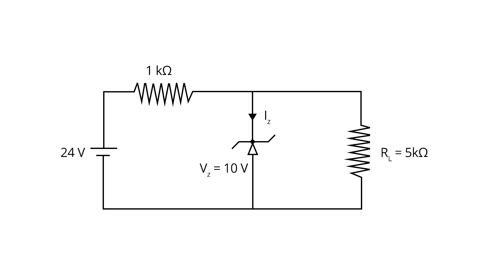
Several advanced devices are based on semiconductor physics, including Zener diodes, LEDs, photodiodes, and solar cells.
A Zener diode operates in reverse breakdown and serves as a voltage regulator. Its voltage relation is $V_z = V_{Z0} + IR_z$.
An LED emits light under forward bias, while a photodiode generates current proportional to light intensity in reverse bias.
Transistors and Their Applications
Transistors are three-terminal devices used as amplifiers, oscillators, and switches. They are made using either the NPN or PNP configuration.
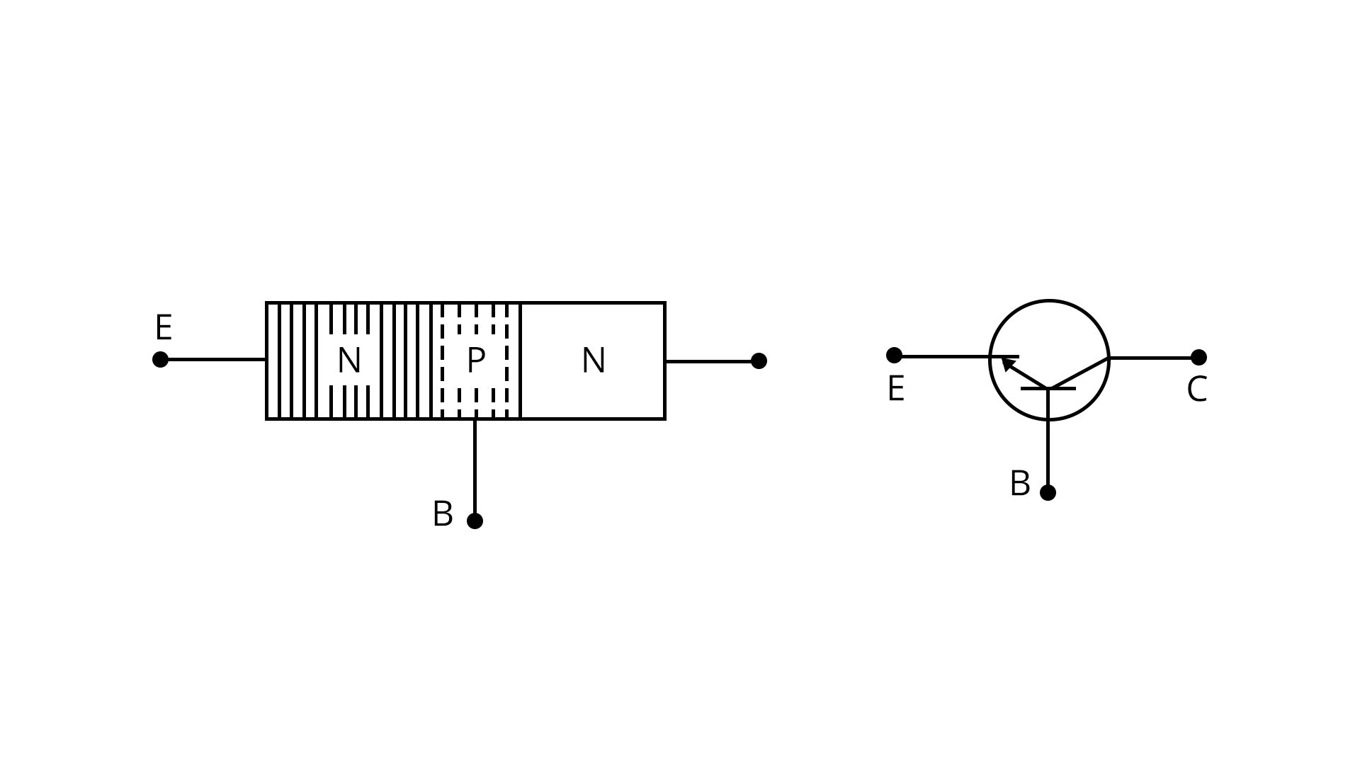
- NPN: Majority charge carriers are electrons
- PNP: Majority charge carriers are holes
In common emitter configuration, the current relations are $I_E = I_C + I_B$. The current gain parameters are $\alpha = \dfrac{I_C}{I_E}$ and $\beta = \dfrac{I_C}{I_B}$.
The voltage gain is $A_v = \dfrac{V_{out}}{V_{in}}$ and, for amplifiers, the detailed voltage gain is $A_v = -\beta \cdot \dfrac{R_c}{R_e + (1+\beta) r_e}$.
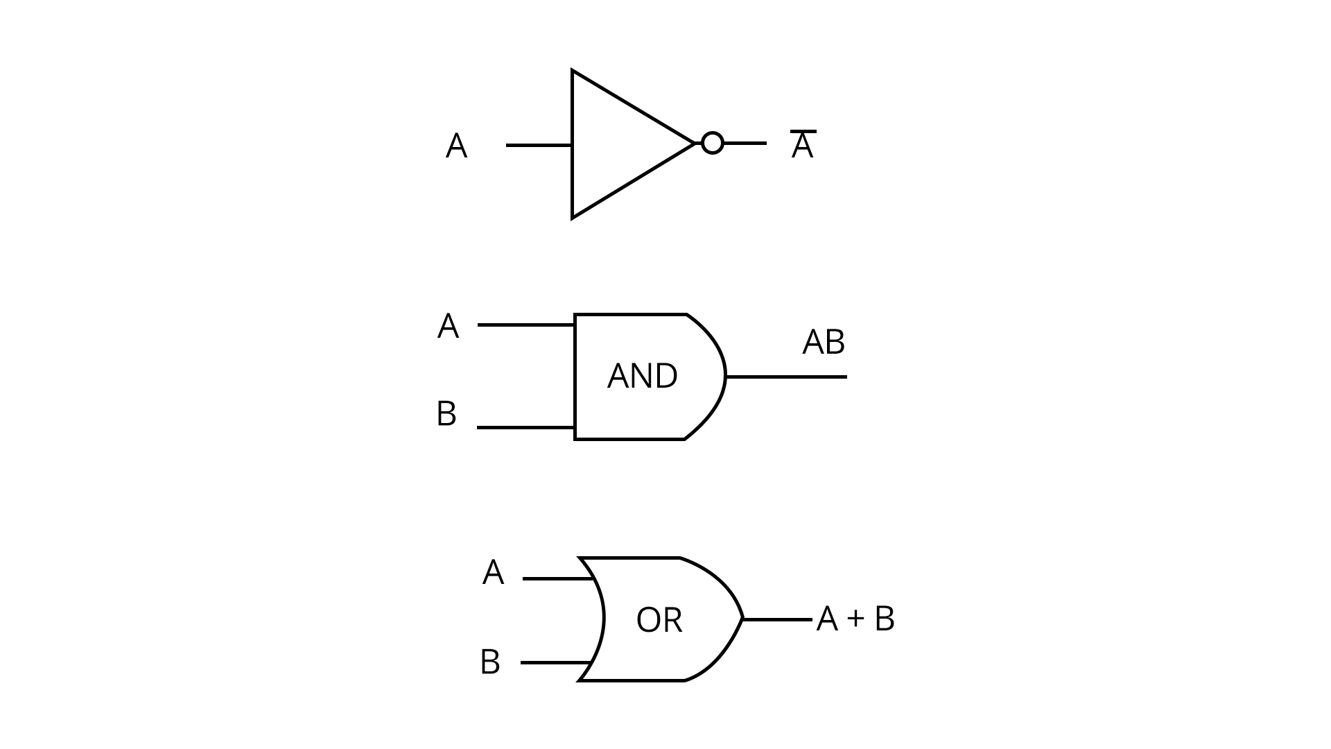
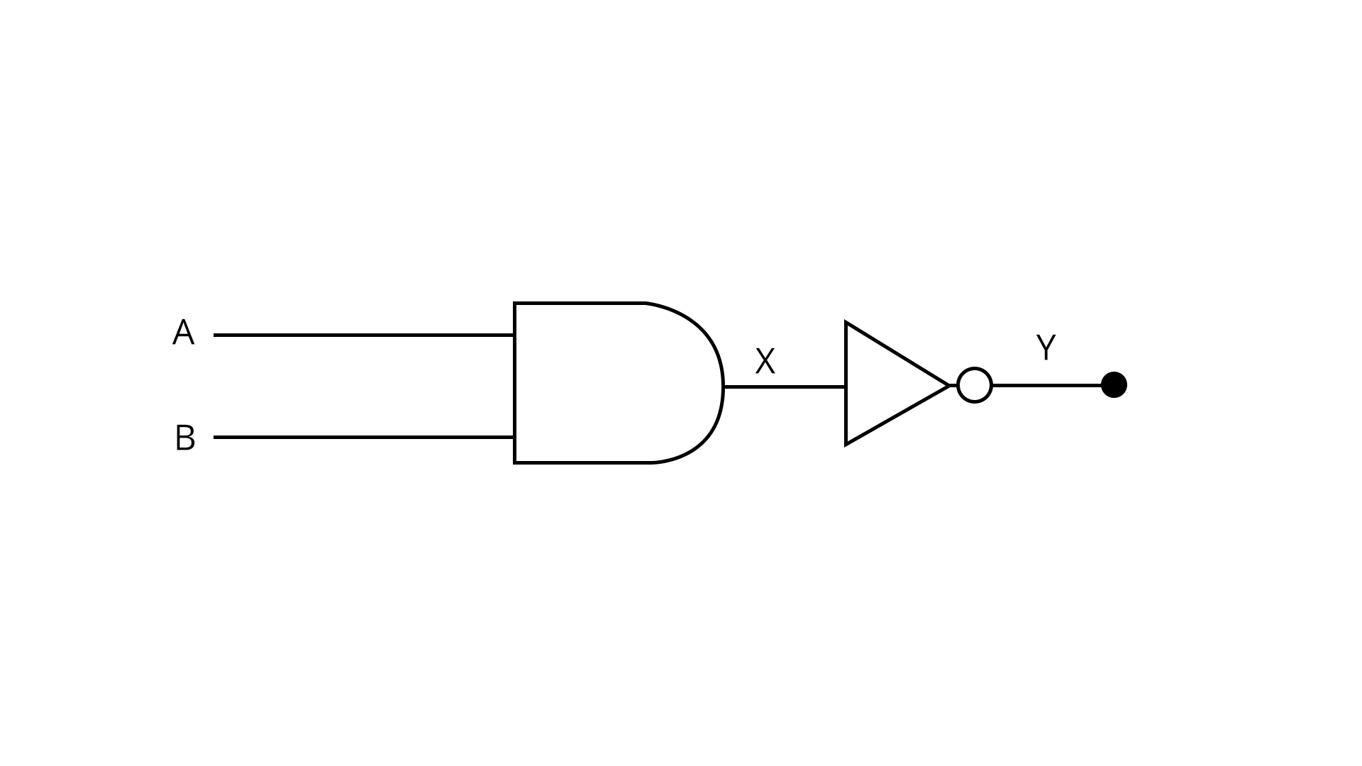
Digital Electronics: Logic Gates
Logic gates form the building blocks of digital devices, performing logical operations on binary inputs. The basic gates are AND, OR, and NOT. Universal gates include NAND and NOR.
De Morgan’s theorems are used to simplify Boolean expressions:
- $\overline{A + B} = \bar{A} \cdot \bar{B}$
- $\overline{A \cdot B} = \bar{A} + \bar{B}$
Truth tables are used to define the output for all input combinations for each logic gate.
Key Formulas in Electronic Devices
| Concept | Formula |
|---|---|
| Mass Action Law | $n_e n_h = n_i^2$ |
| RMS Value of Current | $I_{rms} = \sqrt{I_{dc}^2 + I_{ac}^2}$ |
| Electric Conductivity | $\sigma = e(n_e \mu_e + n_h \mu_h)$ |
| Voltage Gain | $A_v = \dfrac{V_{out}}{V_{in}}$ |
| Current Gain (Transistor) | $\alpha = \dfrac{I_C}{I_E}$, $\beta = \dfrac{I_C}{I_B}$ |
Applications and Further Study
Electronic devices are used in circuits for rectification, amplification, voltage regulation, and digital computation. Their study is essential for deeper understanding of modern electronics and circuit design.
Comprehensive preparation resources, notes, and practice materials are available to support learning in this area on Electronic Devices Overview.
For important problem-solving, refer to Important Questions on Electronic Devices.
Access concise revision resources through Revision Notes for Electronic Devices.
Mock tests for exam simulation are available at Electronic Devices Mock Test. For foundational physics topics, consult the Basic Properties of Electric Charge and Electromagnetic Induction Overview.
Understanding Electronic Devices: Principles and Examples

 Share
Share


FAQs on Understanding Electronic Devices: Principles and Examples
1. What are Electronic Devices?
Electronic devices are components or systems that control, process, and manage the flow of electric current to perform specific functions.
- They mainly use semiconductors like diodes and transistors.
- Applications include communication, computation, signal processing, and control systems.
- Common examples: smartphones, radios, computers, and calculators.
2. What is a semiconductor in electronic devices?
Semiconductors are materials with electrical conductivity between conductors and insulators, crucial for making electronic devices.
- Common semiconductors: Silicon and Germanium.
- They enable the functioning of diodes, transistors, and ICs (integrated circuits).
- Their properties can be controlled by doping with impurities.
3. What is the difference between a diode and a transistor?
A diode allows current to flow in only one direction, while a transistor can amplify and switch electronic signals.
- Diode: Two-terminal device, used mainly for rectification.
- Transistor: Three-terminal device, used for amplification, switching, and signal modulation.
- Both are essential components covered in electronics chapters and exam questions.
4. What are the applications of electronic devices?
Electronic devices have wide applications in various fields.
- Communication devices (mobile phones, radios)
- Computers and laptops
- Medical instruments
- Industrial automation and control systems
- Consumer electronics like TVs and washing machines
5. What is a P-N junction diode and how does it work?
A P-N junction diode is a semiconductor device formed by joining P-type and N-type materials.
- It allows current to flow in one direction only (forward bias).
- In reverse bias, it blocks current flow.
- Used for rectification in power supplies and other circuits.
6. What is meant by doping in semiconductors?
Doping is the process of adding small amounts of impurities to pure semiconductors to change their electrical properties.
- Creates n-type (extra electrons) or p-type (extra holes) materials.
- Doping increases the conductivity of semiconductors, making them useful for electronic devices.
7. What is the principle of a transistor?
The transistor operates by controlling the flow of current between two terminals using a third terminal as a control.
- The three terminals are Emitter, Base, and Collector.
- Works as both an amplifier and a switch in electronic circuits.
- Key for signal processing, covered in most electronics curriculums.
8. What is the function of a rectifier?
A rectifier converts alternating current (AC) into direct current (DC).
- Uses diodes (typically P-N junction diodes).
- Essential for power supplies in electronic devices.
9. What is the importance of logic gates in electronic circuits?
Logic gates are basic building blocks of digital circuits, performing logical operations on one or more binary inputs to produce a single output.
- Main types: AND, OR, NOT, NAND, NOR, etc.
- Used in computers, calculators, memory devices, and more.
10. State the differences between intrinsic and extrinsic semiconductors.
Intrinsic semiconductors are pure, while extrinsic semiconductors are doped with impurities.
- Intrinsic: Pure form, low conductivity.
- Extrinsic: Doped, high conductivity (forms n-type and p-type semiconductors).
- This difference is an important topic for board and competitive exams.
11. What is a Zener diode used for?
A Zener diode is used for voltage regulation in electronic circuits.
- It maintains a constant output voltage despite fluctuations in input.
- Widely used in power supply systems.
12. What are the characteristics of an ideal diode?
An ideal diode allows current to flow only in one direction with zero resistance and blocks all current in reverse direction.
- No forward voltage drop.
- Infinite resistance when reverse-biased.