


How Does Reverse Bias Work? Principles, Diagrams & Key Effects
In Electronics, diode operations mainly revolve around the flow of negatively charged electrons and positively charged holes. In technology, we refer to a semiconductor diode as a pn junction. They play an important role in electronic circuits and make it possible to bring large-sized electronic items to an unimaginable smaller size by their proper use. Biasing is a method of setting a set of proper currents or voltages required for the smooth operation of the circuit or that electronic system, specifically.
We come across two types of biasing in our circuit. One is forward biasing, and the other one is reverse biasing. In a pn junction diode, current carriers flow majorly in only one direction, but if the external voltage applied is in the opposite direction; that condition is said to be reverse biasing.
What is pn Junction Diode?
A pn junction diode is formed when a p-type semiconductor is joined to an n-type semiconductor as a result of which, a potential barrier voltage is developed across the diode junction.
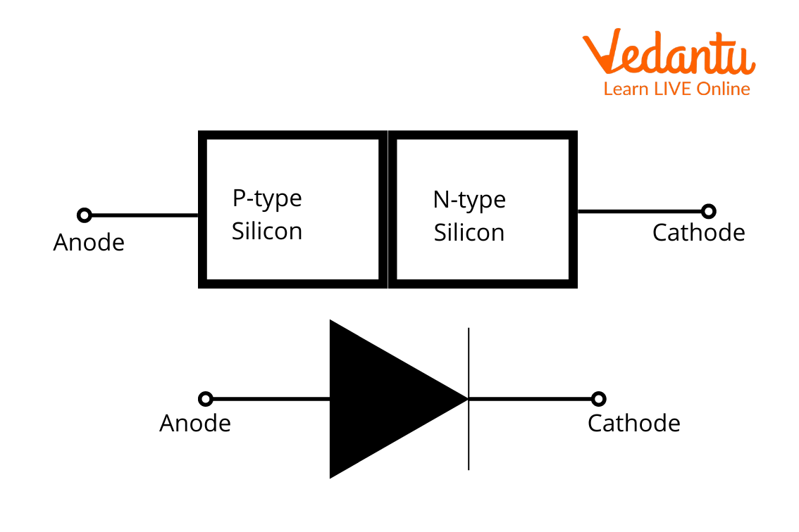
Diode symbol
The depletion region is the space around the boundary of contact between the two diodes, which is formed by the overlapping of positively charged holes and negatively charged electrons, thereby removing any free charge in that region. This is the reason why it is called a depletion region.
History of Inventor
Russell Shoemaker Ohl was an American Scientist born on January 30, 1898. He was the one generally recognized for getting modern Solar Cells patented. He worked a great deal on light-sensitive devices. He was a notable semiconductor researcher before transistors came into being known. He also worked on material research, investigating diode detectors, suitable for military radar, high-frequency wireless and broadcasting.

Russell Shoemaker Ohl
pn Junction Diode Working
Current in a diode flows because of majority and minority charge carriers. In n-type semiconductors, electrons are the majority charge carriers, and holes are the minority charge carriers, whereas in p-type semiconductors, holes are the majority charge carriers and electrons are the minority charge carriers.
Because unlike charge accommodation at the boundary of the junction of the two diodes, a depletion layer is formed which affects charge flow across the diode. When the pn junction is connected across a voltage source, different kinds of flow are observed under different biasing, which we will read below.
pn Junction Diode Characteristics
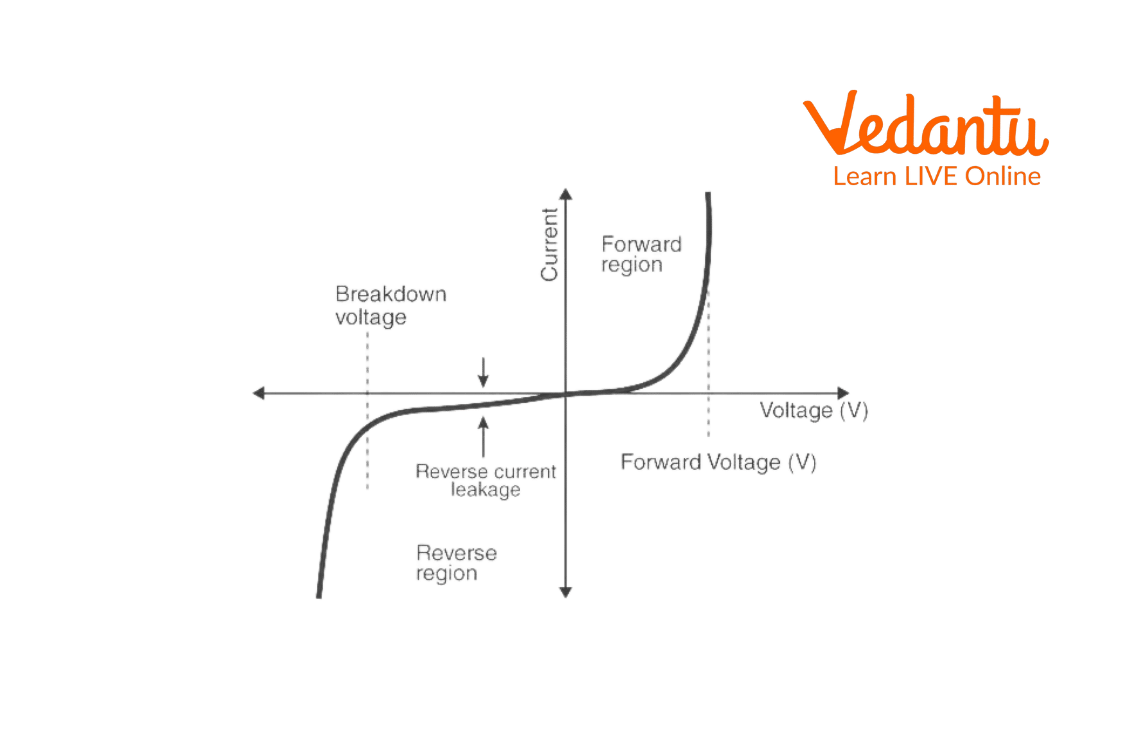
pn junction diode characteristics
Biasing of a Diode
When the pn junction is connected to a battery, it is said to be biased. There are two kinds of bias:
Forward bias diode
Reverse bias diode
Whenever the positive terminal of the battery is connected to the p-type semiconductor and the negative terminal of the battery to n-type semiconductor, the pn junction is said to be forward-biased.
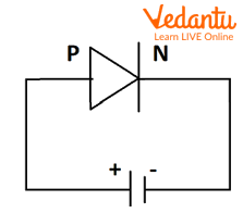
Forward bias
When an n-type semiconductor gets a positive terminal of the battery and a p-type semiconductor gets a negative terminal, pn junction is said to be reverse biased.
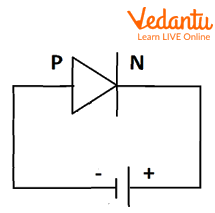
Reverse bias
What is Reverse Bias?
In the reverse bias condition, free electrons diffuse into the p-type region and recombine with the holes, whereas holes diffuse into the n-type semiconductor to combine with electrons. As a result of this, the width of the depletion region increases and no more holes or electrons cross the junction. Even if we supply regulated voltage, no current flows through the diode, hence, pn junctions act like an open switch in case of reverse biasing.
Some Important Questions
1. How does the width of the depletion region get affected in forward and reverse bias?
Ans: Width of the depletion region:
Increases in case of reverse bias
Decreases in case of forwarding bias.
2. How is the Zener diode fabricated for use?
Ans. Zener diodes are made by heavy doping of both p-type and n-type semiconductors. This leads to a decrease in the width of its depletion region, which leads to the production of a large electric field, increasing the current even on applying a high reverse voltage of up to 5V.
3. How is the Zener diode used as a voltage regulator?
Ans.: For large changes in reverse current, the voltage across the Zener diode remains equal to the breakdown voltage because the Zener diode is operated in the reverse breakdown region, therefore, acts like a voltage regulator.
Summary
First, we discussed what a pn junction is, how it operates and how it is made using n-type and p-type semiconductors. Then we read about biasing and its different types, i.e., forward bias and reverse bias. We also discussed the effects of these biasing techniques on the pn junction diode. Next, we read about the inventor of biasing methods, Russel Shoemaker Ohl, an American scientist. Finally, we dealt with some important solved questions based on biasing and pn junction diodes.
List of Related Articles
Forward biasing
FAQs on Reverse Bias in Physics: Explained for Students
1. What is reverse bias in a p-n junction diode?
Reverse bias is a condition where the p-type semiconductor of a diode is connected to the negative terminal of a voltage source, and the n-type semiconductor is connected to the positive terminal. This configuration opposes the natural flow of majority charge carriers, effectively making the diode act like an open switch with very high resistance.
2. How is a p-n junction diode connected in a circuit for reverse bias?
To set up a reverse-biased circuit, the anode (connected to the p-type material) of the diode is connected to the negative end of the DC power supply. The cathode (connected to the n-type material) is then connected to the positive end of the supply. A series resistor is often included to limit the current in case of an accidental breakdown.
3. What are the key differences between forward bias and reverse bias in a diode?
The main differences between forward and reverse bias are:
- Connection: In forward bias, the p-side is connected to the positive terminal and n-side to the negative. In reverse bias, the connection is opposite (p-side to negative, n-side to positive).
- Depletion Region: The width of the depletion region decreases in forward bias, while it increases in reverse bias.
- Resistance: A forward-biased diode offers very low resistance to current flow, whereas a reverse-biased diode offers very high resistance.
- Current Flow: Forward bias allows a large current (in milliamperes) due to majority carriers. Reverse bias allows only a very small leakage current (in microamperes) due to minority carriers.
4. Why is the current in a reverse-biased diode so small and often called 'leakage current'?
The current is extremely small because the applied voltage pulls the majority charge carriers (holes in p-type, electrons in n-type) away from the junction. This widens the depletion region and prevents them from crossing. However, a tiny current still flows due to the movement of minority charge carriers (electrons in the p-side, holes in the n-side), which are pushed across the junction by the applied field. This small, temperature-dependent current is known as reverse saturation current or leakage current.
5. How does the depletion region of a p-n junction change under reverse bias?
Under reverse bias, the external voltage source attracts the majority charge carriers away from the p-n junction. Electrons in the n-region are pulled towards the positive terminal, and holes in the p-region are pulled towards the negative terminal. This movement uncovers more immobile ions at the junction, causing the width of the depletion region to increase and the potential barrier to become higher.
6. What happens if the reverse bias voltage is increased indefinitely? Explain reverse breakdown.
If the reverse bias voltage across a p-n junction is increased to a specific high value, a phenomenon called reverse breakdown occurs. At this point, the diode's high resistance breaks down, and a large current flows through it. This can happen due to two main mechanisms:
- Zener Breakdown: Occurs in heavily doped diodes at lower voltages, where the strong electric field pulls electrons directly from their covalent bonds.
- Avalanche Breakdown: Occurs in lightly doped diodes at higher voltages, where minority carriers gain enough kinetic energy to knock out more carriers through collisions, creating an "avalanche" of charge.
7. What is the diode current equation, and how does it apply to reverse bias?
The ideal diode current equation is given by I = I₀ (e(qV / ηkT) - 1), where I is the diode current, I₀ is the reverse saturation current, and V is the applied voltage. For reverse bias, V is negative and its magnitude is typically much larger than kT/q. This causes the exponential term (e(qV/ηkT)) to approach zero. Therefore, the equation simplifies to I ≈ -I₀, indicating a small, constant reverse saturation current that is independent of the applied voltage.
8. How is the principle of reverse bias used in a Zener diode to regulate voltage?
A Zener diode is a special type of diode designed to operate specifically in the reverse breakdown region. When the reverse voltage across it reaches its 'Zener voltage' (Vz), it breaks down and allows current to flow without being damaged. Crucially, the voltage across the Zener diode remains nearly constant at Vz, even if the current flowing through it changes significantly. This property allows it to be used as a voltage regulator in circuits to provide a stable output voltage from a fluctuating input source.