


What is meant by forwarding bias and reverse bias of the diode? Indicate in a figure.
Answer
629.1k+ views
Hint: In semiconductors doping with acceptor impurities or doping with donor impurities makes the semiconductors more efficient. Both forward bias and reverse bias are the special cases of the P-N junction diode. The joining of the terminals of voltage source with P-type or N-type makes different biases like forward and reverse biases.
Complete step-by-step solution:
Forward bias: If the positive of the voltage terminal joined with the P section is called forward bias.
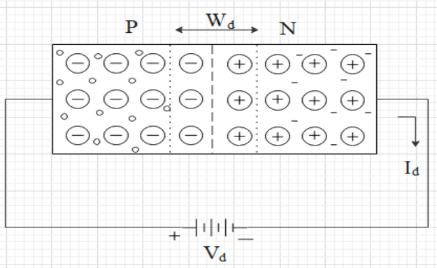
In the forward bias condition the positive voltage is joining with P-type so the positively charged holes repulse towards the depletion layer (\[{{W}_{d}}\]) and the negatively charged electrons repulse towards the depletion layer. The bias potential (\[{{V}_{d}}\]) pressures the holes to recombine with the ions near the depletion layer. The bias potential pressures the electrons to recombine with the ions near the depletion layer So the width of the depletion layer reduces. The applied voltage is equal to the potential barrier then the current (\[{{I}_{d}}\]) produces. At this point the diode current\[{{I}_{d}}=I-{{I}_{s}}\], where \[I\]is current due to majority charge carrier in P section and \[{{I}_{s}}\] is saturation current. Since the potential barrier reduces the electrons attract towards the positive terminal and suddenly the current increases exponentially.
Reverse bias: If the positive of the voltage terminal joined with the N section is called reverse bias.
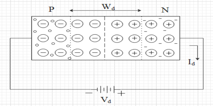
In reverse bias condition, there is an attraction between holes of P-type with negative terminal and the electrons of N-type with a positive terminal. So near the depletion layer the immobile ions are uncovered with holes and electrons, this leads to increases in the depletion layer and increases in potential barrier also. So the majority charge carrier in P-type cannot overcome the potential barrier and electrons also cannot overcome the potential barrier. There is only saturation current that is flowing which is very small (order of \[\mu A\]). So the current \[{{I}_{d}}\] is flowing into the circuit.
Additional Information: There are three possibilities of bias-no bias, forward bias, and reverse bias. Bias means when P-type and N-type join together and the external voltage applied to it is called bias. No bias can say without external voltage or just after the making of the diode. In a semiconductor diode, in the P-type there are holes are majority charge carrier and electrons are minority charge carrier and in N-type, there are electrons are the majority charge carrier and the holes are minority charge carrier.
Note:
(1) In forward bias, the increase in bias potential, the width of the depletion region decrease and the barrier potential also reduces.
(2) In reverse bias, the increase in bias potential, the width of the depletion region increases and the barrier potential also increases.
(3) \[{{({{W}_{d}})}_{rev}}>{{({{W}_{d}})}_{for}}\].
Complete step-by-step solution:
Forward bias: If the positive of the voltage terminal joined with the P section is called forward bias.
In the forward bias condition the positive voltage is joining with P-type so the positively charged holes repulse towards the depletion layer (\[{{W}_{d}}\]) and the negatively charged electrons repulse towards the depletion layer. The bias potential (\[{{V}_{d}}\]) pressures the holes to recombine with the ions near the depletion layer. The bias potential pressures the electrons to recombine with the ions near the depletion layer So the width of the depletion layer reduces. The applied voltage is equal to the potential barrier then the current (\[{{I}_{d}}\]) produces. At this point the diode current\[{{I}_{d}}=I-{{I}_{s}}\], where \[I\]is current due to majority charge carrier in P section and \[{{I}_{s}}\] is saturation current. Since the potential barrier reduces the electrons attract towards the positive terminal and suddenly the current increases exponentially.
Reverse bias: If the positive of the voltage terminal joined with the N section is called reverse bias.
In reverse bias condition, there is an attraction between holes of P-type with negative terminal and the electrons of N-type with a positive terminal. So near the depletion layer the immobile ions are uncovered with holes and electrons, this leads to increases in the depletion layer and increases in potential barrier also. So the majority charge carrier in P-type cannot overcome the potential barrier and electrons also cannot overcome the potential barrier. There is only saturation current that is flowing which is very small (order of \[\mu A\]). So the current \[{{I}_{d}}\] is flowing into the circuit.
Additional Information: There are three possibilities of bias-no bias, forward bias, and reverse bias. Bias means when P-type and N-type join together and the external voltage applied to it is called bias. No bias can say without external voltage or just after the making of the diode. In a semiconductor diode, in the P-type there are holes are majority charge carrier and electrons are minority charge carrier and in N-type, there are electrons are the majority charge carrier and the holes are minority charge carrier.
Note:
(1) In forward bias, the increase in bias potential, the width of the depletion region decrease and the barrier potential also reduces.
(2) In reverse bias, the increase in bias potential, the width of the depletion region increases and the barrier potential also increases.
(3) \[{{({{W}_{d}})}_{rev}}>{{({{W}_{d}})}_{for}}\].
Recently Updated Pages
Master Class 12 Business Studies: Engaging Questions & Answers for Success
Master Class 12 Chemistry: Engaging Questions & Answers for Success
Master Class 12 Biology: Engaging Questions & Answers for Success
Class 12 Question and Answer - Your Ultimate Solutions Guide
Master Class 11 English: Engaging Questions & Answers for Success
Master Class 11 Social Science: Engaging Questions & Answers for Success
Trending doubts
Which are the Top 10 Largest Countries of the World?
Draw a labelled sketch of the human eye class 12 physics CBSE
The end of compass needle which points towards north class 12 physics CBSE
Differentiate between homogeneous and heterogeneous class 12 chemistry CBSE
Why is the cell called the structural and functional class 12 biology CBSE
When was the first election held in India a 194748 class 12 sst CBSE