


How Do Energy Bands Affect Electrical Conductivity?
Energy bands represent the allowed ranges of electron energies in solids, resulting from the interaction and overlap of atomic orbitals in a crystal lattice. The structure of energy bands explains the electrical properties of conductors, semiconductors, and insulators, which is fundamental in solid-state physics and electronic devices.
Formation of Energy Bands in Solids
When atoms form a solid, their outer electron orbitals overlap, leading to a large number of closely spaced energy levels. These closely packed levels merge to form continuous energy bands rather than discrete levels as in isolated atoms.
In a crystal with a large number of atoms (typically on the order of $10^{23}$ per cm$^3$), the splitting of energy levels becomes so fine that bands appear continuous. The precise arrangement and spacing depend on the atomic structure and lattice periodicity.
Types of Energy Bands: Valence, Conduction, and Forbidden Gap
In all crystalline solids, three regions are identified in the energy band structure: the valence band, the conduction band, and the forbidden energy gap. These bands determine the movement of electrons and the resulting electrical properties of a material.
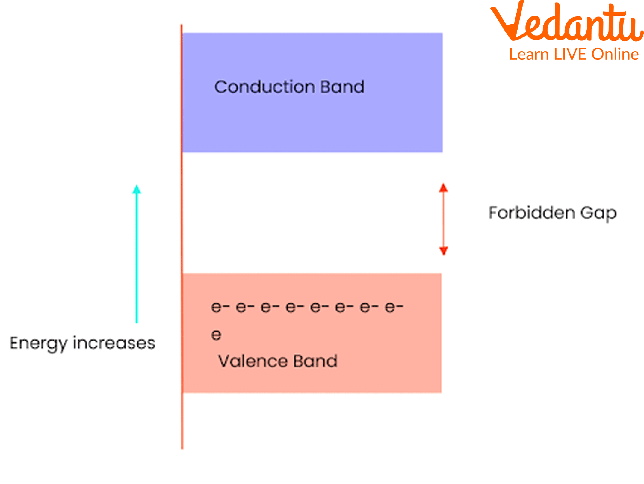
The valence band is the highest energy band completely filled with electrons at absolute zero. Above the valence band lies the conduction band, where electrons can move freely and contribute to electrical conduction. Between these two bands is the forbidden gap (band gap) where no allowed electron states exist.
Classification of Materials Using Energy Bands
The width of the forbidden gap between the valence and conduction bands classifies materials as conductors, semiconductors, or insulators. This feature directly impacts the mobility of electrons and hole charge carriers in different materials.
| Material Type | Energy Band Structure |
|---|---|
| Conductor | Valence and conduction bands overlap; band gap is zero |
| Insulator | Wide forbidden gap (> 5 eV); bands are well separated |
| Semiconductor | Narrow band gap (0.7 – 1.5 eV); partial overlap possible with added energy |
In conductors, such as copper and silver, the valence and conduction bands either overlap or are only slightly separated, permitting free electron motion. Insulators, like glass and diamond, have a wide forbidden gap that prevents electrons from easily moving to the conduction band.
Semiconductors, such as silicon and germanium, possess a small band gap. Thermal or optical excitation can promote electrons from the valence to the conduction band, allowing moderate electrical conduction. For related concepts, refer to Energy Overview.
Valence Band, Conduction Band, and Forbidden Gap Explained
The valence band contains electrons that are generally bound to atoms but can participate in conduction if they acquire sufficient energy. The conduction band is immediately above the valence band and consists of empty or partially filled states where electrons can move freely.
The forbidden gap is an energy interval with no allowed electron states. Its size ($E_g$) is a critical parameter:
- $E_g = 0$ in conductors; electrons move easily
- $E_g \sim 1$ eV in semiconductors; electron excitation possible
- $E_g > 5$ eV in insulators; electron excitation rare
In mathematical terms, the minimum energy required for an electron to move from the valence band to the conduction band is the forbidden energy gap, $E_g$.
Energy Bands in Semiconductors: Intrinsic and Extrinsic Cases
Intrinsic semiconductors, like pure silicon or germanium, have their Fermi level approximately midway between the conduction and valence bands. Electrical conductivity is realized when electrons are thermally excited from the valence band to the conduction band, producing free electrons and holes.
Doping introduces impurities into intrinsic semiconductors to create extrinsic types. n-type semiconductors gain donor atoms, introducing extra energy levels close to the conduction band. p-type semiconductors gain acceptor atoms, with levels near the valence band, altering the material's electrical behavior.
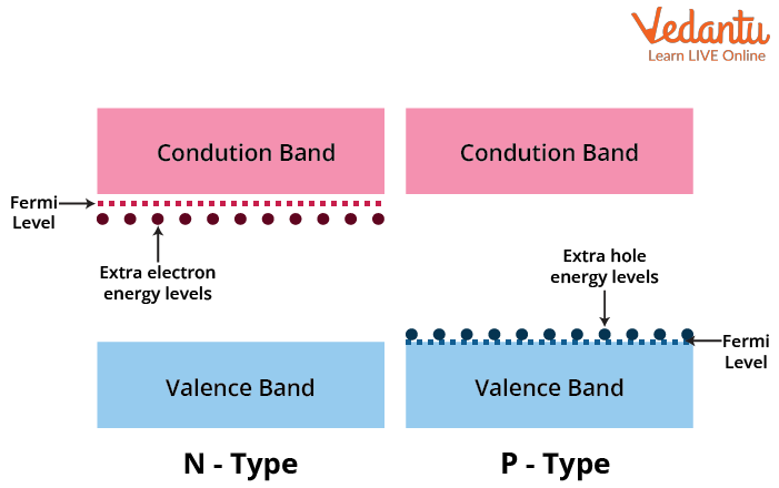
The Fermi level shifts towards the conduction band in n-type materials and towards the valence band in p-type materials, influencing carrier concentration and conductivity.
Energy Bands and Charge Carrier Generation
Electron movement from the valence to the conduction band creates free electrons and corresponding holes. The number of carriers and their dynamics depend on the band gap and the energy provided, such as thermal or optical excitation.
The carrier concentration in semiconductors increases exponentially with temperature, as described by the equation:
$n = N_c \exp\left(-\dfrac{E_g}{2kT}\right)$
where $n$ is the carrier concentration, $N_c$ is the effective density of states, $E_g$ is the band gap, $k$ is Boltzmann’s constant, and $T$ is temperature.
Temperature effects on energy bands and carrier densities are important in semiconductors used in electronic and optoelectronic devices. For practical implications, see Kinetic Energy in Gases.
Applications and Importance of Energy Bands
Understanding energy bands is crucial for the development and operation of electronic components such as diodes, transistors, LEDs, and solar cells. Band gap engineering tailors material properties for specific electronic or photonic functions.
- Determines conduction and insulation properties
- Influences device switching and amplification
- Central to resistance and temperature-dependence calculations
Materials with smaller band gaps require less energy for conduction, making them more suitable for electronic devices. The choice between direct and indirect band gap materials affects optoelectronic efficiency.
Detailed understanding of conduction bands and energy gaps supports circuit design and performance optimization. For thermodynamic considerations, refer to Thermodynamics Basics.
Energy Band Diagram: Solved Example for JEE Main
Given: The energy band gap in silicon is $E_g = 1.1$ eV. If a photon of energy 2 eV is absorbed, it can excite exactly one electron from the valence to the conduction band. Any excess photon energy appears as kinetic energy of the electron.
Example question: If the band gap of a material is 6 eV, identify whether it is a conductor, semiconductor, or insulator.
Solution: A 6 eV band gap is too large for electrons to be excited at room temperature, so the material is classified as an insulator.
Summary of Key Points on Energy Bands
Energy bands arise due to atomic interactions in solids and explain the fundamental electrical properties of materials. The width of the forbidden gap ($E_g$) determines if a material behaves as a conductor, semiconductor, or insulator.
- Conduction occurs through band overlap or narrow gaps
- Insulators have wide forbidden gaps, restricting electron flow
- Semiconductors enable controlled conduction via small band gaps
- Doping modifies band structure and carrier properties
Application of energy band theory is essential for analyzing and designing modern electronic and optoelectronic devices. For further practice, see Practice on Work and Energy.


FAQs on Understanding Energy Bands in Solids
1. What are energy bands in solids?
Energy bands in solids refer to ranges of energy that electrons may occupy due to the overlapping of atomic orbitals in a crystal lattice.
Key points:
- Formed when atoms are closely packed in a solid, causing discrete energy levels to merge.
- Main bands are the valence band (filled with electrons) and the conduction band (higher energy, usually empty).
- The energy band gap separates the two bands, influencing electrical properties.
2. What is the difference between a conductor, semiconductor, and insulator based on energy bands?
The distinction among conductors, semiconductors, and insulators is based on their energy bands and band gap.
- Conductors: Overlapping valence and conduction bands, so electrons flow easily.
- Semiconductors: Small band gap (~1 eV), electrons jump with moderate energy input.
- Insulators: Large band gap (above 3 eV), electrons cannot move to the conduction band easily.
3. What is a band gap?
A band gap (also called forbidden gap) is the energy difference between the top of the valence band and the bottom of the conduction band in a solid.
- Determines if a material is a conductor, semiconductor, or insulator.
- Smaller band gap means higher electrical conductivity.
- Measured in electron volts (eV).
4. Why do energy bands form in solids but not in isolated atoms?
In isolated atoms, electrons have discrete energy levels, but in solids, close-packed atoms cause these levels to overlap and form energy bands.
- Electrons interact with neighboring atoms’ orbitals in solids.
- Levels broaden and merge due to quantum mechanical effects.
- Explains unique electrical behaviors in different types of solids.
5. How does the band theory explain electrical conductivity in semiconductors?
The band theory explains that semiconductors conduct electricity when electrons gain energy to cross the band gap to the conduction band.
- At absolute zero, the conduction band is empty; at room temperature, some electrons jump across the band gap.
- The presence of holes in the valence band also supports conduction.
- Conductivity increases with temperature in semiconductors.
6. What happens to the energy bands of a semiconductor when it is doped?
Doping introduces new energy levels near the conduction or valence band in a semiconductor, changing its electrical properties.
- N-type doping forms donor levels close to the conduction band, increasing free electrons.
- P-type doping forms acceptor levels near the valence band, creating more holes.
- Doping makes conduction easier in semiconductors.
7. What is the significance of the valence band and conduction band?
The valence band and conduction band are key concepts in understanding a solid’s electrical properties.
- The valence band contains electrons involved in bonding.
- The conduction band is where electrons can move freely, enabling conduction.
- The size of the band gap between them determines if the material acts as a conductor, semiconductor, or insulator.
8. Why can metals conduct electricity easily according to band theory?
According to band theory, metals conduct electricity easily because their valence and conduction bands overlap.
- Electrons move freely within the overlapping bands.
- No energy gap (band gap) to prevent electron movement.
- Metals are good electrical conductors as a result.
9. What factors affect the width of the band gap in a material?
The width of the band gap in a material is influenced by several factors.
- The type of atoms and their electronic structure.
- The arrangement and spacing of atoms in the crystal lattice.
- Impurities and dopants added to the material.
- External conditions like pressure and temperature can also have minor effects.
10. What is the importance of energy bands in modern electronics?
Understanding energy bands is crucial for designing electronic devices and materials for modern technology.
- Helps select materials for diodes, transistors, and other components.
- Guides the development of semiconductors and insulators used in circuits.
- Enables innovation in microelectronics, solar cells, and computing hardware.