


What is Common Emitter Configuration Circuit Diagram and Working
The **Common Emitter Configuration** represents one of the most widely used transistor arrangements in electronic circuits, where the emitter terminal serves as the common point between input and output circuits. This configuration provides exceptional current amplification, making it fundamental for signal amplification applications. Understanding its input and output characteristics, circuit diagrams, and operational parameters is essential for designing efficient BJT amplifiers and electronic systems.
Common Emitter Configuration Circuit and Setup
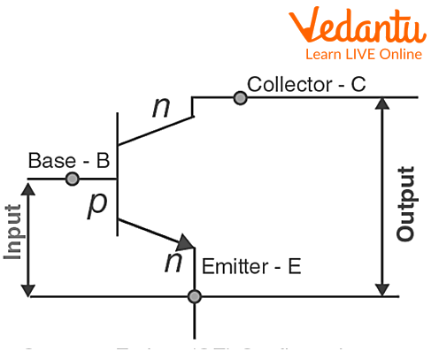
In the common emitter configuration of bjt, the emitter terminal is connected between the collector and base terminals, serving as the reference point for both input and output circuits. The input signal is applied between the base and emitter, while the output is extracted between the collector and emitter terminals.
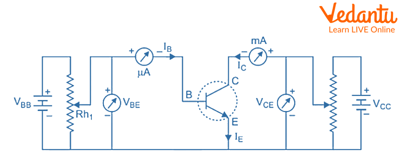
The circuit arrangement utilizes two power supplies: one for biasing the base-emitter junction (forward bias) and another for reverse-biasing the collector-base junction. Variable resistors R1 and R2 control the base current and collector voltage respectively, enabling detailed analysis of transistor behavior.
Base Current Amplification Factor (β)
The base current amplification factor, denoted by β (beta), represents the most crucial parameter of the common emitter configuration. It defines the ratio of collector current to base current in this arrangement.
The relationship between β and α (common base current gain) can be derived through fundamental transistor equations:
- Starting with the basic relation: $I_E = I_B + I_C$
- The common base gain is: $\alpha = \frac{I_C}{I_E}$
- Substituting and rearranging: $\beta = \frac{\alpha}{1-\alpha}$
This relationship demonstrates that as α approaches unity, β approaches infinity, explaining the exceptionally high current gain achievable in common emitter amplifiers.
Collector Current and Circuit Analysis
The collector current in CE configuration depends on both the base current and leakage current. The fundamental equation governing this relationship is:
Where $I_{CEO}$ represents the collector-emitter leakage current with base open. This leakage current becomes significant in high-temperature operations and affects the overall performance of NPN transistor circuits.
Input Characteristics of Common Emitter Configuration
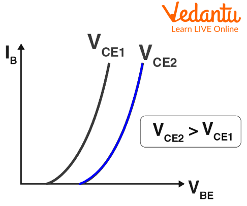
The common emitter configuration input and output characteristics provide comprehensive insight into transistor behavior. The input characteristic curve plots the relationship between base current ($I_B$) and base-emitter voltage ($V_{BE}$) at constant collector-emitter voltage.
Key features of the input characteristic include:
- Exponential increase in base current with increasing $V_{BE}$
- Similar behavior to a forward-biased diode characteristic
- Minimal dependence on collector-emitter voltage variations
Input Resistance Formula: The dynamic input resistance is calculated as:
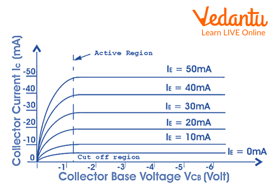
Output Characteristics and Operating Regions
The common emitter configuration output characteristics demonstrate the relationship between collector current ($I_C$) and collector-emitter voltage ($V_{CE}$) for different base current values. This characteristic reveals three distinct operating regions:
FAQs on Common Emitter Configuration of BJT Transistor: Complete Guide
1. What is common emitter configuration in transistor?
Common emitter configuration is a transistor amplifier circuit where the emitter terminal is common to both input and output circuits. In this configuration, the input signal is applied between the base and emitter terminals, while the output is taken from the collector and emitter terminals. Key features include:
- High current gain (β typically 50-200)
- Moderate voltage gain (20-500)
- High power gain due to multiplication of current and voltage gains
- 180° phase shift between input and output signals
- Medium input and output impedance
2. How does a common emitter amplifier work?
A common emitter amplifier works by using a small input current at the base to control a much larger collector current. When a small AC signal is applied to the base-emitter junction:
- Forward bias variation: Input signal varies the forward bias of base-emitter junction
- Base current changes: This causes proportional changes in base current (IB)
- Collector current amplification: Base current changes cause β times larger changes in collector current (IC = β × IB)
- Output voltage generation: Large collector current changes produce amplified output voltage across load resistor
- Signal inversion: Output signal is 180° out of phase with input signal
3. What are the input and output characteristics of CE configuration?
The characteristics of common emitter configuration are represented by two important graphs showing the relationship between currents and voltages:
Input Characteristics (IB vs VBE):
- Shows variation of base current (IB) with base-emitter voltage (VBE)
- Curve is similar to forward-biased diode characteristic
- Knee voltage is approximately 0.7V for silicon and 0.3V for germanium
Output Characteristics (IC vs VCE):
- Shows variation of collector current (IC) with collector-emitter voltage (VCE)
- Contains three regions: saturation, active, and cutoff
- In active region, IC remains nearly constant for different VCE values
4. What is current gain in common emitter configuration?
Current gain in common emitter configuration is the ratio of collector current to base current, denoted by β (beta) or hFE. It represents the current amplification factor of the transistor.
Formula: β = IC/IB
Key points about current gain:
- Typical values: β ranges from 50 to 200 for most transistors
- Temperature dependent: Current gain increases with temperature
- Not constant: Varies slightly with collector current and voltage
- High amplification: Small base current controls large collector current
- Design parameter: Critical for determining amplifier performance
5. What are the advantages of common emitter configuration?
The common emitter configuration offers several advantages making it the most widely used transistor amplifier configuration:
- High current gain: Provides significant current amplification (β = 50-200)
- Good voltage gain: Offers moderate to high voltage amplification
- High power gain: Maximum power amplification among all configurations
- Versatile applications: Suitable for audio, RF, and switching applications
- Easy biasing: Simple biasing circuits can be implemented
- Cost effective: Requires fewer components compared to other configurations
- Wide bandwidth: Acceptable frequency response for most applications
6. What are the disadvantages of common emitter amplifier?
Despite its popularity, the common emitter amplifier has certain limitations that must be considered in circuit design:
- Phase inversion: 180° phase shift between input and output signals
- Temperature sensitivity: Performance varies significantly with temperature changes
- Limited frequency response: Gain decreases at high frequencies due to transistor capacitances
- Input impedance variation: Input resistance changes with operating conditions
- Noise amplification: Amplifies both signal and noise equally
- Stability issues: May require feedback for stable operation
- Distortion: Non-linear characteristics can introduce harmonic distortion