


(a) Draw the circuit diagram of a full-wave rectifier using a p-n junction diode. Explain its working and show the output, input waveforms.
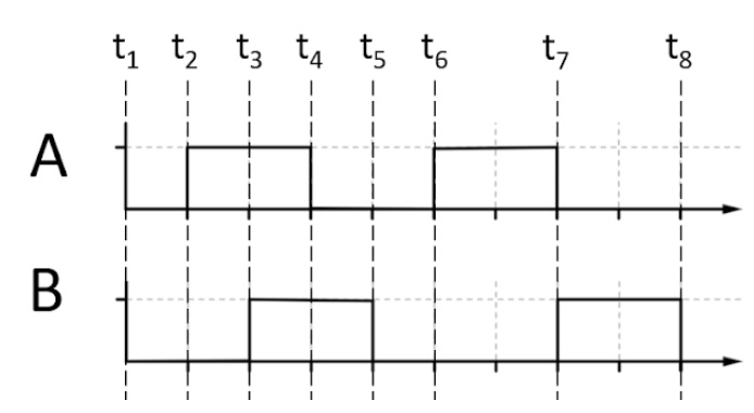
(b) Show the output waveforms (Y) for the following inputs A and B of (i) OR gate (ii) NAND gate
Answer
592.2k+ views
Hint: For the first part we will first make the diagram of the full-wave rectifier and then we will explain how a full-wave rectifier works as well as draw the input and output waves for it. In the second part, we will calculate the output of the given A and B waves when they are passed through an OR gate and a NAND gate.
Complete step-by-step solution:
First, we will draw the circuit diagram of a full-wave rectifier using the p-n junction diode.
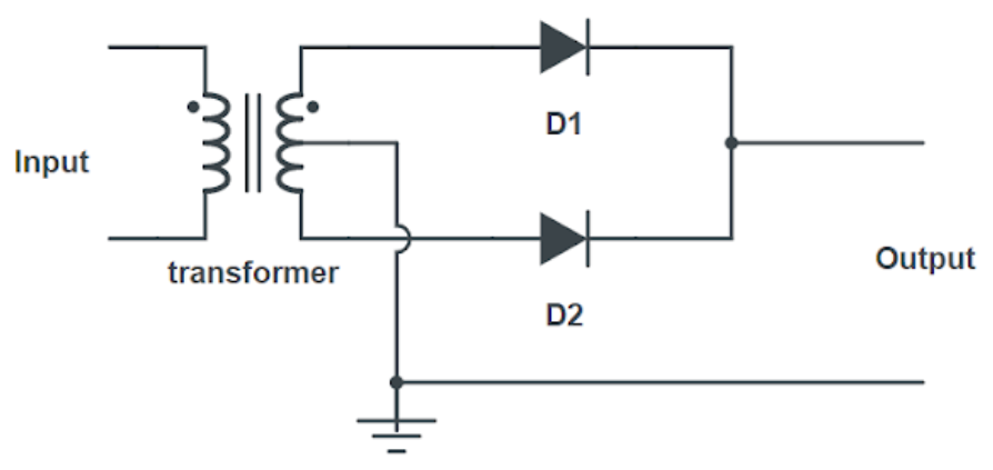
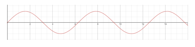
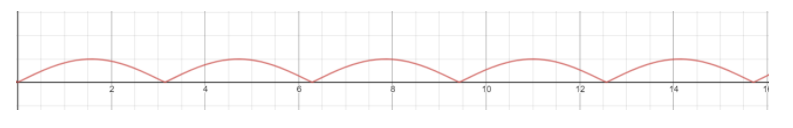
In the diagram, we can see that we need two p-n junction diodes and a center-tap transformer. In this, we have used a center-tap transformer. The potential at the center tap will be zero as it is earthed. And suppose at one moment, the potential towards the D1 diode will be positive and towards the D2 diode will be negative. The only current through D1 will pass and for the next half-cycle when the polarity of input reverses, the potential will be positive towards D2 and the current will pass through it. So, we will get the complete cycle in positive. Hence, the name full-wave rectifier. Let us take a sampled sine wave input and the output it will give in the full-wave rectifier.
Input:
Output:
Now for the second part. We will calculate Y for the given gates and the given waves A and B.
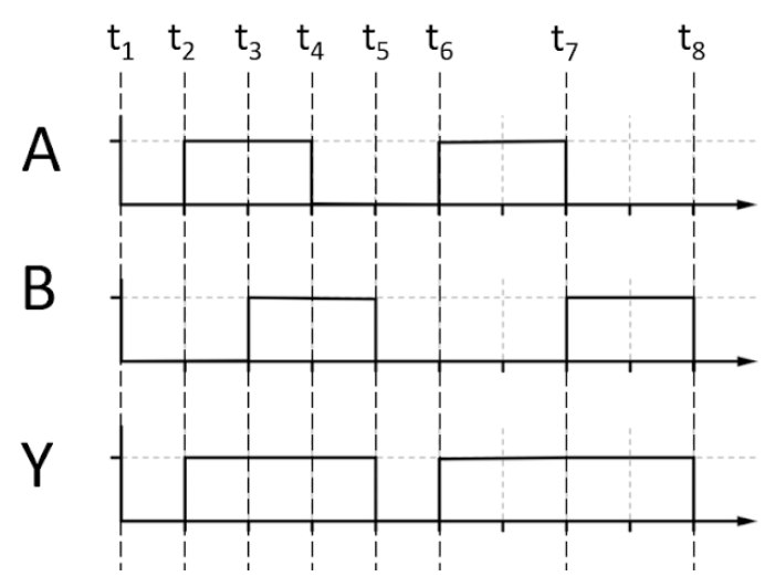
For the OR gate, if either of the signals is 1 in any of the intervals then the output wave, Y will also be 1 in that interval.
For the NAND gate, we will first get the output wave for the AND gate. For the AND gate both the inputs need to be 1 for the output to be 1.
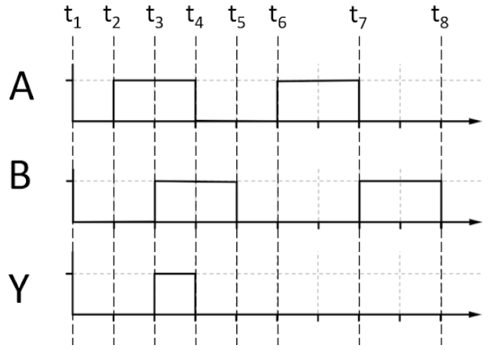
And the output for the NAND gate will be the inverse of that of the AND gate.
Note: Observe that the output maximum potential difference is half of that of the input wave. This happens because we use the center tap transformer wherein the middle is earthed so only half of the potential difference between the edges gets transferred to the output. Take care of time intervals when calculating Y for the different gates.
Complete step-by-step solution:
First, we will draw the circuit diagram of a full-wave rectifier using the p-n junction diode.
In the diagram, we can see that we need two p-n junction diodes and a center-tap transformer. In this, we have used a center-tap transformer. The potential at the center tap will be zero as it is earthed. And suppose at one moment, the potential towards the D1 diode will be positive and towards the D2 diode will be negative. The only current through D1 will pass and for the next half-cycle when the polarity of input reverses, the potential will be positive towards D2 and the current will pass through it. So, we will get the complete cycle in positive. Hence, the name full-wave rectifier. Let us take a sampled sine wave input and the output it will give in the full-wave rectifier.
Input:
Output:
Now for the second part. We will calculate Y for the given gates and the given waves A and B.
For the OR gate, if either of the signals is 1 in any of the intervals then the output wave, Y will also be 1 in that interval.
For the NAND gate, we will first get the output wave for the AND gate. For the AND gate both the inputs need to be 1 for the output to be 1.
And the output for the NAND gate will be the inverse of that of the AND gate.
Note: Observe that the output maximum potential difference is half of that of the input wave. This happens because we use the center tap transformer wherein the middle is earthed so only half of the potential difference between the edges gets transferred to the output. Take care of time intervals when calculating Y for the different gates.
Recently Updated Pages
Master Class 12 Economics: Engaging Questions & Answers for Success
Master Class 12 Physics: Engaging Questions & Answers for Success
Master Class 12 English: Engaging Questions & Answers for Success
Master Class 12 Social Science: Engaging Questions & Answers for Success
Master Class 12 Maths: Engaging Questions & Answers for Success
Master Class 12 Business Studies: Engaging Questions & Answers for Success
Trending doubts
Which are the Top 10 Largest Countries of the World?
What are the major means of transport Explain each class 12 social science CBSE
Draw a labelled sketch of the human eye class 12 physics CBSE
Why cannot DNA pass through cell membranes class 12 biology CBSE
Differentiate between insitu conservation and exsitu class 12 biology CBSE
Draw a neat and well labeled diagram of TS of ovary class 12 biology CBSE