


With a neat diagram, explain the working of a single stage CE amplifier. Draw the frequency response curve and discuss the results.
Answer
602.7k+ views
Hint: Before knowing about the single stage CE amplifiers one should know about the basic concepts on amplifiers, types of amplifiers, about transistors and some basics about biasing.
Complete step by step answer
When only one transistor associated with the circuit is used for amplification of a weak signal, the circuit is known as a single-stage amplifier. When a common emitter base is used to collect the amplified signal it is known as the single stage CE amplifier.
The diagram of a single stage CE amplifier is given below
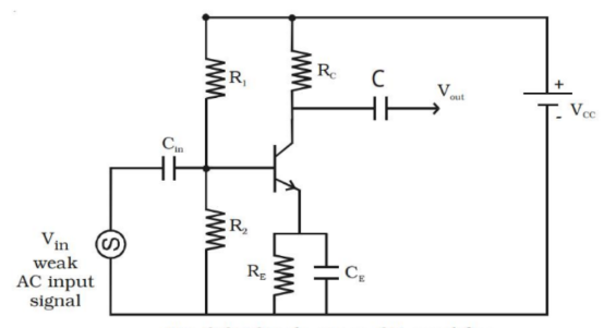
A simple stage CE amplifier has different circuit elements and functions. Let us discuss about that,
The resistance $ {R_1},{R_2},{R_E} $ shown in the diagram forms the biasing circuit.
The circuit used to couple the signal to the base of the transistor is known as the input capacitance, $ {C_{in}} $ circuit. The signal source resistance will come across $ {R_2} $ if this circuit is not used, and thus change the bias. The capacitor $ {C_{in}} $ allows only a.c. signal to flow through it
The capacitor connected in parallel with RE to provide a low reactance path to the amplified AC signal is known as the Emitter bypass capacitor CE. If this capacitor is not used, then the amplified AC signal flowing through RE will cause a voltage drop across it, thereby shifting the output voltage.
The capacitor used to couple the amplified signal to the output device is known as coupling capacitor C. This capacitor C allows only a.c. signal to flow through it
Working:
A small base current flows when a weak input a.c. signal is given to the base of the transistor. A much larger a.c. current flows through collector load RC due to transistor action. A large voltage appears across RC and hence we get a large voltage at the output. Therefore, a weak signal applied to the base came out in amplified form in the collector circuit. The ratio of the amplified output voltage to the input voltage in the amplifier is known as the Voltage gain (Av) of the amplifier.
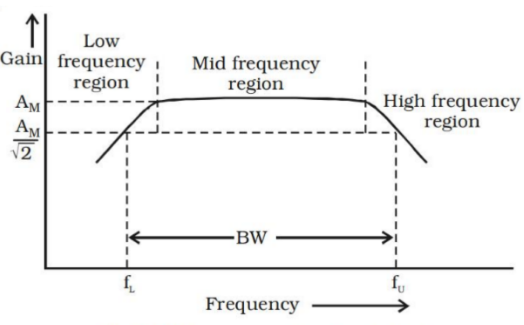
The above diagram shows the frequency response curve
The voltage gain (Av) of the amplifier for different input frequencies can be determined using the frequency response graph. Taking frequency (f) along X–axis and voltage gain (Av) along Y–axis a graph is drawn. The frequency response curve obtained from the graph it will be like the one which is shown in the diagram above
It is seen that the amplifier gain decreases at very low frequency and at very high frequency, but over a wide range of mid frequency regions it remains constant. The frequency in the low frequency range at which the gain of the amplifier is $ \dfrac{1}{{\sqrt 2 }} $ times the mid frequency gain (AM) is known as the lower cut off frequency.
The frequency in the high frequency range at which the gain of the amplifier is $ \dfrac{1}{{\sqrt 2 }} $ times the mid frequency gain (AM) is known as the upper cut of frequency.
The frequency interval between lower cut off and upper cutoff frequencies is known as the Bandwidth of the single stage CE amplifier.
$ BW = {f_u} - {f_l} $
Where,
BW is the bandwidth
$ {f_u} $ is the upper cut of frequency.
$ {f_l} $ is the lower cut off frequency.
Note
The single stage CE amplifier is used in the initial stages of public address (PA) amplifier systems, in stereo amplifiers, in tape recorder, CD players, VCRs, DVD players, in radio and television receivers and most widely used as a voltages amplifier.
Complete step by step answer
When only one transistor associated with the circuit is used for amplification of a weak signal, the circuit is known as a single-stage amplifier. When a common emitter base is used to collect the amplified signal it is known as the single stage CE amplifier.
The diagram of a single stage CE amplifier is given below
A simple stage CE amplifier has different circuit elements and functions. Let us discuss about that,
The resistance $ {R_1},{R_2},{R_E} $ shown in the diagram forms the biasing circuit.
The circuit used to couple the signal to the base of the transistor is known as the input capacitance, $ {C_{in}} $ circuit. The signal source resistance will come across $ {R_2} $ if this circuit is not used, and thus change the bias. The capacitor $ {C_{in}} $ allows only a.c. signal to flow through it
The capacitor connected in parallel with RE to provide a low reactance path to the amplified AC signal is known as the Emitter bypass capacitor CE. If this capacitor is not used, then the amplified AC signal flowing through RE will cause a voltage drop across it, thereby shifting the output voltage.
The capacitor used to couple the amplified signal to the output device is known as coupling capacitor C. This capacitor C allows only a.c. signal to flow through it
Working:
A small base current flows when a weak input a.c. signal is given to the base of the transistor. A much larger a.c. current flows through collector load RC due to transistor action. A large voltage appears across RC and hence we get a large voltage at the output. Therefore, a weak signal applied to the base came out in amplified form in the collector circuit. The ratio of the amplified output voltage to the input voltage in the amplifier is known as the Voltage gain (Av) of the amplifier.
The above diagram shows the frequency response curve
The voltage gain (Av) of the amplifier for different input frequencies can be determined using the frequency response graph. Taking frequency (f) along X–axis and voltage gain (Av) along Y–axis a graph is drawn. The frequency response curve obtained from the graph it will be like the one which is shown in the diagram above
It is seen that the amplifier gain decreases at very low frequency and at very high frequency, but over a wide range of mid frequency regions it remains constant. The frequency in the low frequency range at which the gain of the amplifier is $ \dfrac{1}{{\sqrt 2 }} $ times the mid frequency gain (AM) is known as the lower cut off frequency.
The frequency in the high frequency range at which the gain of the amplifier is $ \dfrac{1}{{\sqrt 2 }} $ times the mid frequency gain (AM) is known as the upper cut of frequency.
The frequency interval between lower cut off and upper cutoff frequencies is known as the Bandwidth of the single stage CE amplifier.
$ BW = {f_u} - {f_l} $
Where,
BW is the bandwidth
$ {f_u} $ is the upper cut of frequency.
$ {f_l} $ is the lower cut off frequency.
Note
The single stage CE amplifier is used in the initial stages of public address (PA) amplifier systems, in stereo amplifiers, in tape recorder, CD players, VCRs, DVD players, in radio and television receivers and most widely used as a voltages amplifier.
Recently Updated Pages
Master Class 12 Business Studies: Engaging Questions & Answers for Success
Master Class 12 Chemistry: Engaging Questions & Answers for Success
Master Class 12 Biology: Engaging Questions & Answers for Success
Class 12 Question and Answer - Your Ultimate Solutions Guide
Master Class 11 English: Engaging Questions & Answers for Success
Master Class 11 Social Science: Engaging Questions & Answers for Success
Trending doubts
Which are the Top 10 Largest Countries of the World?
Draw a labelled sketch of the human eye class 12 physics CBSE
Differentiate between homogeneous and heterogeneous class 12 chemistry CBSE
In order to find out the different types of gametes class 12 biology NEET_UG
Why is the cell called the structural and functional class 12 biology CBSE
Draw ray diagrams each showing i myopic eye and ii class 12 physics CBSE