


Zener diode is used in reverse bias. When its reverse bias is increased, how does the thickness of the depletion layer change?
Answer
536.7k+ views
Hint: A zener diode is a heavily doped diode. The junction potential of the zener diode increases as the zener diode is connected in reverse biased condition. When the reverse biased voltage increases across the zener diode the width of the depletion layer increases.
Complete step-by-step solution:
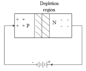
The zener diode always operates in reverse biased condition. That is, when the reverse biased voltage increases across the zener diode the width of the depletion layer increases. As a result the width of the depletion layer becomes wider. This also reduces the majority carrier current across the zener diode. And on the other hand minority current carriers increase. We have already said that when the reverse biased voltage increases across the zener diode the width of the depletion layer increases. But there is a limit in which the depletion layer can widen. Whenever the limit is crossed once there will be rapid increase in current with the small increase in voltage.
Therefore when the reverse biased voltage increases across the zener diode the width of the depletion layer increases.
Note: A zener diode is a heavily doped diode. For a wide range of current the breakdown voltage for a zener diode will be a constant. When a zener diode is used in the forward biased condition it will act as a normal diode. For a Silicon diode the width of the depletion layer ranges for a micrometer to tens of micrometer.
Complete step-by-step solution:
The zener diode always operates in reverse biased condition. That is, when the reverse biased voltage increases across the zener diode the width of the depletion layer increases. As a result the width of the depletion layer becomes wider. This also reduces the majority carrier current across the zener diode. And on the other hand minority current carriers increase. We have already said that when the reverse biased voltage increases across the zener diode the width of the depletion layer increases. But there is a limit in which the depletion layer can widen. Whenever the limit is crossed once there will be rapid increase in current with the small increase in voltage.
Therefore when the reverse biased voltage increases across the zener diode the width of the depletion layer increases.
Note: A zener diode is a heavily doped diode. For a wide range of current the breakdown voltage for a zener diode will be a constant. When a zener diode is used in the forward biased condition it will act as a normal diode. For a Silicon diode the width of the depletion layer ranges for a micrometer to tens of micrometer.
Recently Updated Pages
Master Class 12 Business Studies: Engaging Questions & Answers for Success
Master Class 12 Chemistry: Engaging Questions & Answers for Success
Master Class 12 Biology: Engaging Questions & Answers for Success
Class 12 Question and Answer - Your Ultimate Solutions Guide
Master Class 11 Social Science: Engaging Questions & Answers for Success
Master Class 11 Chemistry: Engaging Questions & Answers for Success
Trending doubts
Which are the Top 10 Largest Countries of the World?
Draw a labelled sketch of the human eye class 12 physics CBSE
Name the crygenes that control cotton bollworm and class 12 biology CBSE
Differentiate between homogeneous and heterogeneous class 12 chemistry CBSE
Ribosomal RNA is actively synthesised in A Nucleoplasm class 12 biology CBSE
How many molecules of ATP and NADPH are required information class 12 biology CBSE