


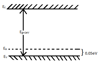
What is the type of the semiconductor, for the energy band diagram shown in the figure?
$ \left( A \right) $ N-type semiconductor
$ \left( B \right) $ P-type semiconductor
$ \left( C \right) $ Intrinsic semiconductor
$ \left( D \right) $ Both N and P type semiconductor
Answer
543.6k+ views
Hint: To solve the given question we need to recall the energy band diagram of N-type, P-type and intrinsic semiconductor device. We will also know what are N-type semiconductors, P-type semiconductors and intrinsic semiconductors.
Complete step by step answer:
First of all we will know what is meant by semiconductor. Semiconductors are the material whose conductivity (how much electricity can flow through the material) lies between conductors and insulators.
Now, we will know about the P-type semiconductor devices. We know that when p and n type semiconductors combine, a depletion region is formed due to the recombination of electrons of n region with holes of p region. The density of holes in the p-type region is known as acceptor density and the density of holes in the N-type region is known as donor density. When the acceptor density is more than the donor density the pn junction becomes a P-type semiconductor device. P-type semiconductor is doped with trivalent impurity. Therefore one excessive whole is created and hence, the acceptor density increases. So here the Acceptor level is near the valence band.
When the donor density is more than the acceptor density the pn junction becomes an N-type semiconductor device. N-type semiconductor is doped with pentavalent impurity. Therefore one excessive electron is created and hence, the donor density increases. So here the Acceptor level is near the conduction band.
Intrinsic semiconductor devices are also known as pure semiconductor devices. In intrinsic semiconductors there is no doping. So there is no free charge carrier and the conduction band is initially empty but when some energy is provided to the electrons, they start jumping to the conduction band and hence result in conductivity. The Acceptor level in pure semiconductor devices lies in between the valence and conduction band.
Here, if we see the given energy band diagram and compare the three types of semiconductor devices then we will know that the given diagram represents a P-type semiconductor.
Hence, option $ \left( B \right) $ is the correct answer.
Note:
One must keep in mind the position of the Acceptor level while solving such a question. If the acceptor level was near the conduction band then the energy band diagram would be representing N-type semiconductor device, if the acceptor level was in between then it would represent intrinsic semiconductor and if the acceptor level was constant but two conduction band and valence band were at different position then it would represent both p and n type semiconductor.
Recently Updated Pages
Master Class 12 Social Science: Engaging Questions & Answers for Success
Master Class 12 Physics: Engaging Questions & Answers for Success
Master Class 12 Maths: Engaging Questions & Answers for Success
Master Class 12 Economics: Engaging Questions & Answers for Success
Master Class 12 Chemistry: Engaging Questions & Answers for Success
Master Class 12 Business Studies: Engaging Questions & Answers for Success
Trending doubts
Which are the Top 10 Largest Countries of the World?
Draw a labelled sketch of the human eye class 12 physics CBSE
Explain the structure of megasporangium class 12 biology CBSE
What are the major means of transport Explain each class 12 social science CBSE
How many chromosomes are found in human ovum a 46 b class 12 biology CBSE
The diagram of the section of a maize grain is given class 12 biology CBSE