


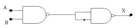
The output (X) of the logic circuit shown in figure will be
$\begin{align}
& \left( a \right)X=A.B \\
& \left( b \right)X=\overline{A+B} \\
& \left( c \right)X=\overline{\overline{A}}.\overline{\overline{B}} \\
& \left( d \right)X=\overline{A.B} \\
\end{align}$
Answer
567k+ views
Hint: All other digital circuits are made up of these three basic logic gates. Hence, NAND gate is a combination of AND and NOT gate. In other words, output of AND gate is connected to the input of NOT gate. Thus the output of NAND gate is opposite to AND gate. When two inputs of a NAND gate are shorted, the resulting circuit acts as a NOT gate. Hence in the given figure the output of the first NAND gate is connected to a NOT gate and the resulting output will be the output from that NOT gate.
Complete answer:
A logic gate is a digital circuit with one or input signal but only one output signal. There are three basic logic gates. All digital circuits are made with these three gates. That is, AND gate, OR gate and NOT gate.
An OR gate is a logic circuit that has two or more inputs but only one output. The output of an OR gate is high, if any or all the inputs are high. Similarly, AND gate is a logic circuit that has two or more inputs and one output. The output of an AND gate shows high when all the inputs are high. However, the output of the AND gate is low if any or all inputs are low. NOT gate or inverter is the simplest of all logic gates. It has only one input and one output. Thus the NOT gate is an inverter.
All other digital circuits are made up of these three basic logic gates. Hence, NAND gate is a combination of AND and NOT gate. In other words, output of AND gate is connected to the input of NOT gate. Thus the output of NAND gate is opposite to AND gate.
The Boolean expression of NAND gate is,
$X=\overline{A.B}$
where, $X=A.B$ is the Boolean expression of AND gate and Y is the output.
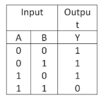
Truth table of NAND gate given by,
NAND gate is a universal gate because its repeated use can produce other logic gates like AND, OR and NOT.
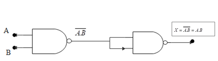
Here from the figure $\overline{A.B}$ is the output of NAND gate and then it is connected to an inverter. Thus,
$X=\overline{\overline{A.B}}=A.B$
Hence, the output of the entire logic circuit acts as an AND gate.
Therefore option (a) is correct.
Note:
All other digital circuits are made up of these three basic logic gates. Hence, NAND gate is a combination of AND and NOT gate. In other words, output of AND gate is connected to the input of NOT gate. Thus the output of NAND gate is opposite to AND gate. NAND gate is a universal gate because its repeated use can produce other logic gates like AND, OR and NOT.
Complete answer:
A logic gate is a digital circuit with one or input signal but only one output signal. There are three basic logic gates. All digital circuits are made with these three gates. That is, AND gate, OR gate and NOT gate.
An OR gate is a logic circuit that has two or more inputs but only one output. The output of an OR gate is high, if any or all the inputs are high. Similarly, AND gate is a logic circuit that has two or more inputs and one output. The output of an AND gate shows high when all the inputs are high. However, the output of the AND gate is low if any or all inputs are low. NOT gate or inverter is the simplest of all logic gates. It has only one input and one output. Thus the NOT gate is an inverter.
All other digital circuits are made up of these three basic logic gates. Hence, NAND gate is a combination of AND and NOT gate. In other words, output of AND gate is connected to the input of NOT gate. Thus the output of NAND gate is opposite to AND gate.
The Boolean expression of NAND gate is,
$X=\overline{A.B}$
where, $X=A.B$ is the Boolean expression of AND gate and Y is the output.
Truth table of NAND gate given by,
NAND gate is a universal gate because its repeated use can produce other logic gates like AND, OR and NOT.
Here from the figure $\overline{A.B}$ is the output of NAND gate and then it is connected to an inverter. Thus,
$X=\overline{\overline{A.B}}=A.B$
Hence, the output of the entire logic circuit acts as an AND gate.
Therefore option (a) is correct.
Note:
All other digital circuits are made up of these three basic logic gates. Hence, NAND gate is a combination of AND and NOT gate. In other words, output of AND gate is connected to the input of NOT gate. Thus the output of NAND gate is opposite to AND gate. NAND gate is a universal gate because its repeated use can produce other logic gates like AND, OR and NOT.
Recently Updated Pages
Master Class 12 Economics: Engaging Questions & Answers for Success
Master Class 12 Physics: Engaging Questions & Answers for Success
Master Class 12 English: Engaging Questions & Answers for Success
Master Class 12 Social Science: Engaging Questions & Answers for Success
Master Class 12 Maths: Engaging Questions & Answers for Success
Master Class 12 Business Studies: Engaging Questions & Answers for Success
Trending doubts
Which are the Top 10 Largest Countries of the World?
What are the major means of transport Explain each class 12 social science CBSE
Draw a labelled sketch of the human eye class 12 physics CBSE
Why cannot DNA pass through cell membranes class 12 biology CBSE
Differentiate between insitu conservation and exsitu class 12 biology CBSE
Draw a neat and well labeled diagram of TS of ovary class 12 biology CBSE