


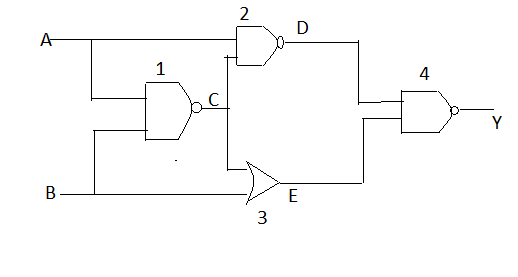
The output of the given logic circuit is:
A.$\bar{A}B$
B.$A\bar{B}$
C.$AB+A\bar{B}$
D.$A\bar{B}+\bar{A}B$
Answer
593.7k+ views
Hint: To solve this problem we need to discuss about the output of NAND gate and NOT gate which are used in the above diagram, further we will use de Morgan’s theorem, commutative, commutative and associative properties of Boolean algebra to solve the logic gates equations.
Complete answer:
First we will see the properties of NAND gate,
Truth table for NAND gate is given as,
The output for NAND gate is negation of output of AND gate which is given by $\overline{A\cdot B}$.
By de Morgan’s theorem we have,
$\Rightarrow \overline{A\cdot B}=\overline{A}+\overline{B}$
So the output from the gate 1 will be
$\Rightarrow C=\overline{A}+\overline{B}$
Now for gate 2 input will be A and $\overline{A}+\overline{B}$ so by the above table of NAND gate we have,
$\Rightarrow \overline{\overline{A}+\overline{B}}$
Or by de Morgan’s law
$\Rightarrow D=\overline{A}+\bar{B}$
Now for gate 3, which is OR gate truth table is,
For OR gate if either input one or input two is true the output will be true ,
Now from the above diagram by taking input C and B for or gate we have,
$\Rightarrow E=C+B=\overline{A}+\overline{B}+B$
$\Rightarrow E=\overline{A}$
Now for the final gate which is NAND gate the inputs will be D and E SO,
$\Rightarrow Y=\overline{D.E}$
By putting the values of D and E and applying de Morgan’s law in some steps we have,
$\Rightarrow Y=\overline{\overline{(A}+\overline{B})\overline{A}}$
$\Rightarrow Y=\overline{\overline{A}+\overline{A}B}$
$\Rightarrow Y=A\overline{(\overline{A}B)}$
$\Rightarrow Y=A(A+\overline{B})$
$\Rightarrow Y=A+A\overline{B}=A\overline{B}$
$\Rightarrow Y=A\overline{B}$
$\therefore $ The output of the given logic gate diagram will be $A\overline{B}$, hence option B is correct
Note:
In these type of circuit in which different type of multiple logic gates are used we need to carefully calculate the output of each logic gate step by step and store its value in some variable, so it can be act as a input for next logic gate, and to avoid any type of mistakes it's better to write down the truth table of each logic gate involved. Try to minimize the equations with the help of Boolean properties and theorems of logic gates.
Complete answer:
First we will see the properties of NAND gate,
Truth table for NAND gate is given as,
| A | B | $\overline{A\cdot B}$ |
| 0 | 0 | 1 |
| 0 | 1 | 1 |
| 1 | 0 | 1 |
| 1 | 1 | 0 |
The output for NAND gate is negation of output of AND gate which is given by $\overline{A\cdot B}$.
By de Morgan’s theorem we have,
$\Rightarrow \overline{A\cdot B}=\overline{A}+\overline{B}$
So the output from the gate 1 will be
$\Rightarrow C=\overline{A}+\overline{B}$
Now for gate 2 input will be A and $\overline{A}+\overline{B}$ so by the above table of NAND gate we have,
$\Rightarrow \overline{\overline{A}+\overline{B}}$
Or by de Morgan’s law
$\Rightarrow D=\overline{A}+\bar{B}$
Now for gate 3, which is OR gate truth table is,
| C | B | C+B |
| 0 | 0 | 0 |
| 0 | 1 | 1 |
| 1 | 0 | 1 |
| 1 | 1 | 1 |
For OR gate if either input one or input two is true the output will be true ,
Now from the above diagram by taking input C and B for or gate we have,
$\Rightarrow E=C+B=\overline{A}+\overline{B}+B$
$\Rightarrow E=\overline{A}$
Now for the final gate which is NAND gate the inputs will be D and E SO,
$\Rightarrow Y=\overline{D.E}$
By putting the values of D and E and applying de Morgan’s law in some steps we have,
$\Rightarrow Y=\overline{\overline{(A}+\overline{B})\overline{A}}$
$\Rightarrow Y=\overline{\overline{A}+\overline{A}B}$
$\Rightarrow Y=A\overline{(\overline{A}B)}$
$\Rightarrow Y=A(A+\overline{B})$
$\Rightarrow Y=A+A\overline{B}=A\overline{B}$
$\Rightarrow Y=A\overline{B}$
$\therefore $ The output of the given logic gate diagram will be $A\overline{B}$, hence option B is correct
Note:
In these type of circuit in which different type of multiple logic gates are used we need to carefully calculate the output of each logic gate step by step and store its value in some variable, so it can be act as a input for next logic gate, and to avoid any type of mistakes it's better to write down the truth table of each logic gate involved. Try to minimize the equations with the help of Boolean properties and theorems of logic gates.
Recently Updated Pages
Master Class 12 Business Studies: Engaging Questions & Answers for Success
Master Class 12 Chemistry: Engaging Questions & Answers for Success
Master Class 12 Biology: Engaging Questions & Answers for Success
Class 12 Question and Answer - Your Ultimate Solutions Guide
Master Class 11 English: Engaging Questions & Answers for Success
Master Class 11 Social Science: Engaging Questions & Answers for Success
Trending doubts
Which are the Top 10 Largest Countries of the World?
Draw a labelled sketch of the human eye class 12 physics CBSE
The end of compass needle which points towards north class 12 physics CBSE
Differentiate between homogeneous and heterogeneous class 12 chemistry CBSE
In order to find out the different types of gametes class 12 biology NEET_UG
Why is the cell called the structural and functional class 12 biology CBSE