


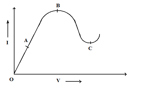
The graph shown in the figure represents a plot of current versus voltage for a given semiconductor. Identify the region, if any, over which the semiconductor has negative resistance.
Answer
605.4k+ views
Hint: Conductors can be classified according to Ohm’s law of resistance. The conductors which obey Ohm’s law are ohmic conductors, they always have positive value of resistance. The conductors which don’t obey Ohm’s law are called non-ohmic conductors. Semiconductors are non-ohmic in nature.
Complete step by step answer:
We all have heard about Ohm’s law. Ohm’s law states that at a constant temperature, current flowing through a conductor is directly proportional to the potential difference across two ends of the conductor.
Mathematically, $I \propto V$
Where, $I$ is current flowing through a conductor
$V$ is the potential difference across two ends of the conductor.
Resistance is the proportionality constant in the expression of Ohm’s law, which in turn is the opposition offered by the conductor to the flow of electric current through it. It is represented by the symbol $R$.
Thus the expression for Ohm’s law becomes,
$V = IR$
Slope of the current versus voltage graph can be used to calculate the resistance of any type of conductor. For an ohmic conductor, the $VI - $ graph is a straight line.
So slope of the line represents the value of resistance, that is, $R = \dfrac{V}{I}$.
For non-ohmic conductors, like vacuum tubes, semiconductors, transistors etcetera, the
$VI - $ graph is a curved line showing both negative and positive resistance associated with them.
Slope of the tangent at any point can be calculated and taken as the value of resistance in these non-ohmic conductors.
Resistance of non-ohmic conductors is given by,
$R = \dfrac{{\Delta V}}{{\Delta I}}$
Where, $\Delta V$ is the relative potential difference.
$\Delta I$ is the value of the relative amount of current.
In the provided graph, the region between points B and C shows negative relative amounts of current, implying negative value of resistance.
Therefore the region between points B and C have negative value of resistance for the given semiconductor.
Note: Notice the unit of current provided is in $milli - Amperes.$ which means semiconductors are able to only carry a small amount of current with a very large potential difference. It is due to the fact that in a forward-biased semiconductor, the majority of charge carriers move away from the junction so the effective resistance across the junction is so high. This results in a very low amount of current flow across a comparatively large potential difference.
Recently Updated Pages
Master Class 12 Economics: Engaging Questions & Answers for Success
Master Class 12 English: Engaging Questions & Answers for Success
Master Class 12 Social Science: Engaging Questions & Answers for Success
Master Class 12 Maths: Engaging Questions & Answers for Success
Master Class 12 Physics: Engaging Questions & Answers for Success
Master Class 12 Business Studies: Engaging Questions & Answers for Success
Trending doubts
Which are the Top 10 Largest Countries of the World?
Draw a labelled sketch of the human eye class 12 physics CBSE
Differentiate between homogeneous and heterogeneous class 12 chemistry CBSE
Why is the cell called the structural and functional class 12 biology CBSE
Draw ray diagrams each showing i myopic eye and ii class 12 physics CBSE
Which is the correct genotypic ratio of mendel dihybrid class 12 biology CBSE