


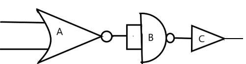
The circuit is as shown in the figure. The equivalent gate is –
A) NOR gate
B) OR gate
C) AND gate
D) NAND gate
Answer
596.4k+ views
Hint: We are given a combination of logical gates. We have to devise the output of this entire system. We know that this can be easily done using the Boolean algebra or the binary operation on the binary digits 0 and 1. We need to draw the truth tables for each logical gate.
Complete step by step answer:
We can convert the given combination of logical gates into a single system of logical gates. We can employ the techniques in Boolean algebra for the same. We know that the logic gates are simply, the unary or binary operations done on the binary digits. The main three operations are the AND, the OR and the NOT. Each has its own function and symbolic representation.
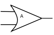
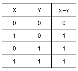
OR gate: The OR gate or the logical OR is the binary operation which produces a truth table such that its output is true, if at least one of the inputs is true (or 1). It is represented by the symbol –
Its truth table looks like –
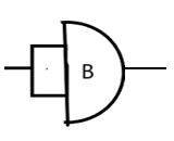
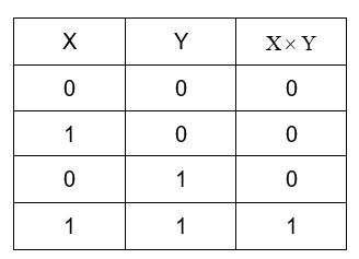
AND gate: The AND gate or the logical AND is the binary operation which produces a truth table such that its output is true (or 1), if and only if both the inputs are true. It is represented by the symbol -
Its truth table looks like –
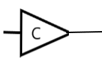
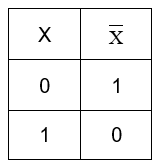
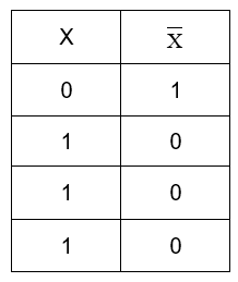
NOT gate: The NOT logical gate is the negation operation in logical operations. It gives the output negated as that of its input. It is a unary operation. It is represented by the symbol –
The truth table of NOT gate looks like –
A circle or dot in the front of any other operation denotes a NOT operation along with it, i.e., NAND or NOR.
Now, let us consider the given circuit. A is a NOR, B is a NAND and C is NOT operation.

We can draw the truth tables for each of the logical gates.
For the gate A,
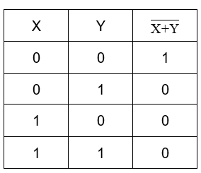
Now, the inputs of gate B are the outputs from the gate A,
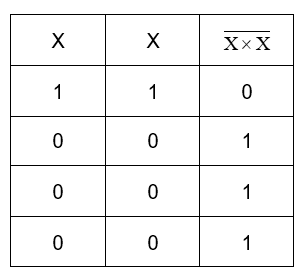
Now we can employ the gate C as –
We have the output of the whole circuit as in the above truth table. When we compare it with the truth tables of the logical operations, we realise that the negation of AND gate gives this result. So, the required equivalent gate is NAND.
The correct answer is option D.
Note:
We can convert most of the complicated logic gate circuits into easy basic operations by using this technique. This technique is widely used in electrical and electronic designing which gives a very efficient method to design the circuits involved.
Complete step by step answer:
We can convert the given combination of logical gates into a single system of logical gates. We can employ the techniques in Boolean algebra for the same. We know that the logic gates are simply, the unary or binary operations done on the binary digits. The main three operations are the AND, the OR and the NOT. Each has its own function and symbolic representation.
OR gate: The OR gate or the logical OR is the binary operation which produces a truth table such that its output is true, if at least one of the inputs is true (or 1). It is represented by the symbol –
Its truth table looks like –
AND gate: The AND gate or the logical AND is the binary operation which produces a truth table such that its output is true (or 1), if and only if both the inputs are true. It is represented by the symbol -
Its truth table looks like –
NOT gate: The NOT logical gate is the negation operation in logical operations. It gives the output negated as that of its input. It is a unary operation. It is represented by the symbol –
The truth table of NOT gate looks like –
A circle or dot in the front of any other operation denotes a NOT operation along with it, i.e., NAND or NOR.
Now, let us consider the given circuit. A is a NOR, B is a NAND and C is NOT operation.
We can draw the truth tables for each of the logical gates.
For the gate A,
Now, the inputs of gate B are the outputs from the gate A,
Now we can employ the gate C as –
We have the output of the whole circuit as in the above truth table. When we compare it with the truth tables of the logical operations, we realise that the negation of AND gate gives this result. So, the required equivalent gate is NAND.
The correct answer is option D.
Note:
We can convert most of the complicated logic gate circuits into easy basic operations by using this technique. This technique is widely used in electrical and electronic designing which gives a very efficient method to design the circuits involved.
Recently Updated Pages
Master Class 12 Business Studies: Engaging Questions & Answers for Success
Master Class 12 Biology: Engaging Questions & Answers for Success
Master Class 12 Chemistry: Engaging Questions & Answers for Success
Class 12 Question and Answer - Your Ultimate Solutions Guide
Master Class 11 Social Science: Engaging Questions & Answers for Success
Master Class 11 English: Engaging Questions & Answers for Success
Trending doubts
Which is more stable and why class 12 chemistry CBSE
What are the major means of transport Explain each class 12 social science CBSE
Name the part of the flower which the tassels of the class 12 biology CBSE
The value of constant k in coulombs law is beginalign class 12 physics CBSE
Suicide bags of cells are aEndoplasmic reticulum bLysosome class 12 biology CBSE
Quantisation of charge implies a Charge does not exist class 12 physics CBSE