


The barrier potential of a silicon diode is
A. 0.3V
B. 0.7V
C. 1.1V
D. -0.7V
Answer
636.3k+ views
Hint: Recall how we make a p-n junction diode. And about the movement of the majority charge carriers results in the formation of the depletion layer and corresponding a potential difference is created between the two terminals, the potential barrier. For silicon, it is 0.7V.
Complete step-by-step answer:
Potential barrier: The diode is an electronic device that acts as a switch in a circuit. It will allow the movement of current in one direction. Usually, diodes are made with doped semiconductors. Generally, in electronic circuits, p-n junction diodes are used. When a p-type semiconductor and an n-type semiconductor are fused, we get a p-n junction diode. An n-type semiconductor has a high concentration of electrons.
So, we can say the electrons are majority charge carriers, and holes are the minority charge carriers. Whereas in p types, holes are majority charge carriers and electrons are minority charge carriers. Remember the material on which this p-type and n-type are fabricated should belong to the same type of semiconductor.
P- n junction potential barrier:
After the fusing of these two types of conductors, what happens is, majority charge carriers in n-type that is the electrons will start to move towards the p-type semiconductor. It is a diffusion process. Similarly, the holes will seem to move from the left (p) end to the right (n) end.
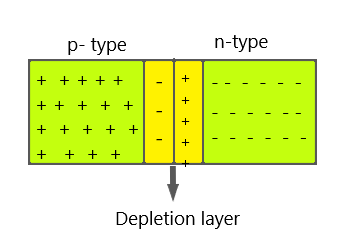
After some electrons and holes are drifted towards the other side through the junction, a depletion layer is created at the intersection of the two semiconductors. That is, the region near the junction of n-type is blocked with holes and that of p-type with electrons. Then the electrons will not move freely towards the p region and vice versa due to this layer.
Some external force is needed to push electrons towards the right side. A potential difference is created between the two terminals. That potential difference is nothing but the potential barrier. This varies by the type of semiconductor material, doping and temperature.
To overcome the potential barrier, electrons and holes must need some voltage which should be equal to or greater than the potential barrier. As I mentioned, each semiconductor has a potential barrier.
In the case of silicon, its potential barrier is 0.7V. That means if we need to work a silicon diode, then we must apply a voltage of minimum 0.7V to make it work.
Note: Since the majority charge carriers are electrons in the n-type conductor, the total charge is negative, hence the name n-type. And similarly, for p-type. Remember, after crossing the potential barrier electron-hole recombination takes place. Since the electrons move from n to p, the direction of the flow of electric current will be from p to n.
Complete step-by-step answer:
Potential barrier: The diode is an electronic device that acts as a switch in a circuit. It will allow the movement of current in one direction. Usually, diodes are made with doped semiconductors. Generally, in electronic circuits, p-n junction diodes are used. When a p-type semiconductor and an n-type semiconductor are fused, we get a p-n junction diode. An n-type semiconductor has a high concentration of electrons.
So, we can say the electrons are majority charge carriers, and holes are the minority charge carriers. Whereas in p types, holes are majority charge carriers and electrons are minority charge carriers. Remember the material on which this p-type and n-type are fabricated should belong to the same type of semiconductor.
P- n junction potential barrier:
After the fusing of these two types of conductors, what happens is, majority charge carriers in n-type that is the electrons will start to move towards the p-type semiconductor. It is a diffusion process. Similarly, the holes will seem to move from the left (p) end to the right (n) end.
After some electrons and holes are drifted towards the other side through the junction, a depletion layer is created at the intersection of the two semiconductors. That is, the region near the junction of n-type is blocked with holes and that of p-type with electrons. Then the electrons will not move freely towards the p region and vice versa due to this layer.
Some external force is needed to push electrons towards the right side. A potential difference is created between the two terminals. That potential difference is nothing but the potential barrier. This varies by the type of semiconductor material, doping and temperature.
To overcome the potential barrier, electrons and holes must need some voltage which should be equal to or greater than the potential barrier. As I mentioned, each semiconductor has a potential barrier.
In the case of silicon, its potential barrier is 0.7V. That means if we need to work a silicon diode, then we must apply a voltage of minimum 0.7V to make it work.
Note: Since the majority charge carriers are electrons in the n-type conductor, the total charge is negative, hence the name n-type. And similarly, for p-type. Remember, after crossing the potential barrier electron-hole recombination takes place. Since the electrons move from n to p, the direction of the flow of electric current will be from p to n.
Recently Updated Pages
Master Class 12 Economics: Engaging Questions & Answers for Success
Master Class 12 English: Engaging Questions & Answers for Success
Master Class 12 Social Science: Engaging Questions & Answers for Success
Master Class 12 Maths: Engaging Questions & Answers for Success
Master Class 12 Physics: Engaging Questions & Answers for Success
Master Class 12 Business Studies: Engaging Questions & Answers for Success
Trending doubts
Which are the Top 10 Largest Countries of the World?
Draw a labelled sketch of the human eye class 12 physics CBSE
Differentiate between homogeneous and heterogeneous class 12 chemistry CBSE
Why is the cell called the structural and functional class 12 biology CBSE
Draw ray diagrams each showing i myopic eye and ii class 12 physics CBSE
Which is the correct genotypic ratio of mendel dihybrid class 12 biology CBSE