


What happens to the potential barrier of the p- n junction diode when it is?
Answer
590.7k+ views
Hint: Diode is the type of the semiconductor material that is used as the switch to allow the current in one direction and restricting the current flowing in the opposite direction. Out of which the p- n junction diode (positive- negative) is most commonly used.
Complete step by step solution:
The p- n junction diode has two terminals which are formed as the p type semiconductor and the n type semiconductor joins. The p type semiconductor has the positive holes as the majority charge carriers and the n- type semiconductor has the majority electric electron as the charge carriers. This diode functions only when the diode is forward biased. But if the diode is reverse biased, the current does not flow through the circuit.
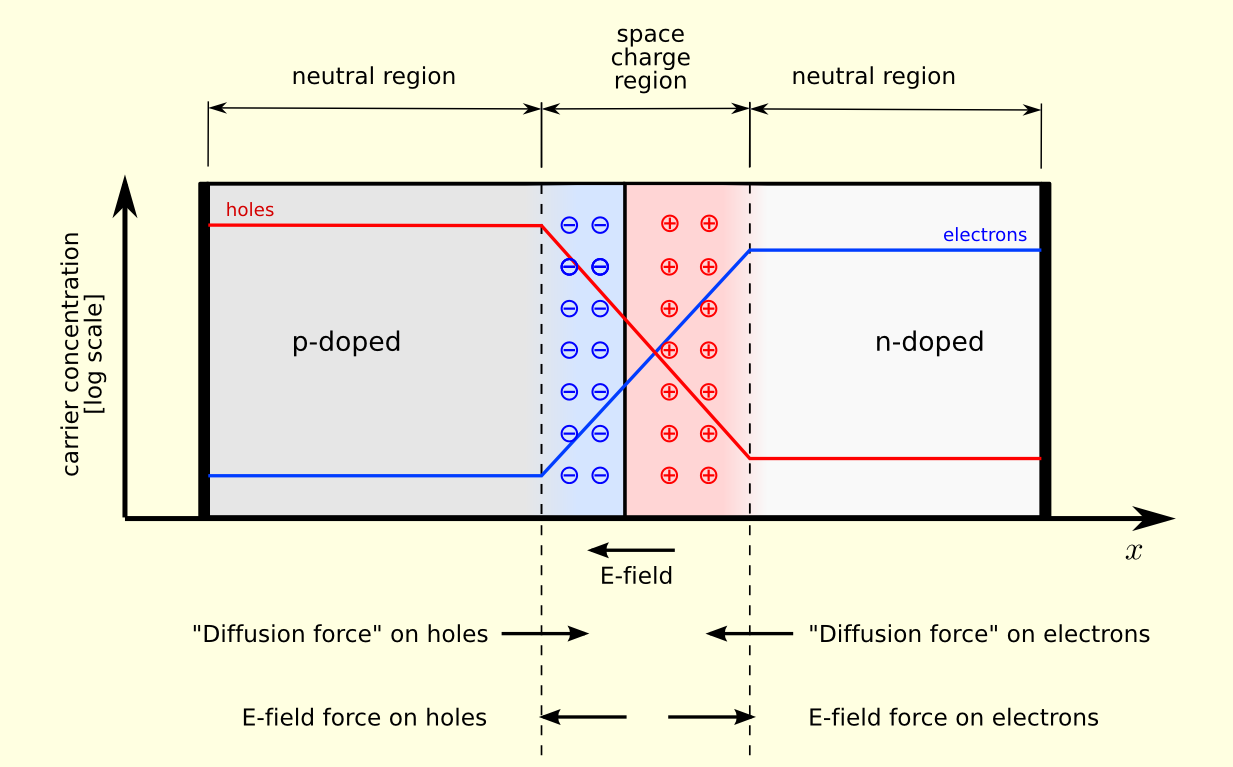
When the current passes, the negative terminal releases the electrons and these electrons move towards the positive terminal and thus it reduces the depletion region by reducing potential barrier. In a p- n junction diode, the potential barrier is $0.7\,V$ if silicon is used. After breaking the barrier, the conventional current flows through the circuit. Hence the electrons flow through the negative terminal and holes to the positive terminal.
Note: The material that makes up the p- n semiconductor is silicon, germanium and the gallium arsenide. Out of which the silicon semiconductor is most commonly used, this is because the silicon can withstand the higher temperature during the flow of the charged particles than the germanium semiconductor.
Complete step by step solution:
The p- n junction diode has two terminals which are formed as the p type semiconductor and the n type semiconductor joins. The p type semiconductor has the positive holes as the majority charge carriers and the n- type semiconductor has the majority electric electron as the charge carriers. This diode functions only when the diode is forward biased. But if the diode is reverse biased, the current does not flow through the circuit.
When the current passes, the negative terminal releases the electrons and these electrons move towards the positive terminal and thus it reduces the depletion region by reducing potential barrier. In a p- n junction diode, the potential barrier is $0.7\,V$ if silicon is used. After breaking the barrier, the conventional current flows through the circuit. Hence the electrons flow through the negative terminal and holes to the positive terminal.
Note: The material that makes up the p- n semiconductor is silicon, germanium and the gallium arsenide. Out of which the silicon semiconductor is most commonly used, this is because the silicon can withstand the higher temperature during the flow of the charged particles than the germanium semiconductor.
Recently Updated Pages
Master Class 12 Social Science: Engaging Questions & Answers for Success
Master Class 12 Physics: Engaging Questions & Answers for Success
Master Class 12 Maths: Engaging Questions & Answers for Success
Master Class 12 Economics: Engaging Questions & Answers for Success
Master Class 12 Chemistry: Engaging Questions & Answers for Success
Master Class 12 Business Studies: Engaging Questions & Answers for Success
Trending doubts
Which are the Top 10 Largest Countries of the World?
Draw a labelled sketch of the human eye class 12 physics CBSE
Explain the structure of megasporangium class 12 biology CBSE
What are the major means of transport Explain each class 12 social science CBSE
How many chromosomes are found in human ovum a 46 b class 12 biology CBSE
The diagram of the section of a maize grain is given class 12 biology CBSE