


For the action of a CE transistor, (E=emitter, B= base, C= collector) the required CB, EB junction bias conditions are:
$(a)$ both EB and CB junctions forward bias
$(b)$ both EB and CB junctions reverse bias
$(c)$ EB junction forward bias, CB junction reverse bias
$(d)$ EB junction reverse bias, CB junction forward bias
Answer
630k+ views
- Hint: In this question use the concept that in CE configuration an emitter is common for both the input as well as the output circuit. For proper functioning of this CE configuration the EB that is emitter base junction must be forward biased with the help of a diode. This will help approaching the problem statement.
Complete step-by-step answer:
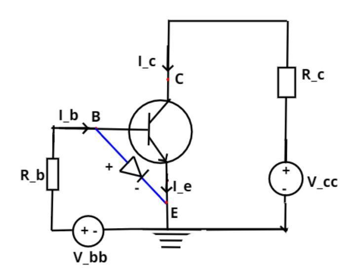
In a common emitter configuration the emitter is worked as a mediator i.e. it is connected to collector as well as base of the CE transistor.
The pictorial representation of an n – p – n transistor is shown above.
Now the transistor to work the base emitter (BE) junction is always forward biased by a diode.
If the diode is made of silicon then the BE voltage is 0.7
Therefore,${V_{BE}}$ = 0.7V.
If the diode is made up of germanium then the BE voltage is 0.2
Therefore, ${V_{BE}}$ = 0.2V.
So for the action of the CE transistor BE junction is always forward biased.
And for the action of the CE transistor Collector base (CB) junction there is always reverse bias.
So this is the required answer.
Hence option (C) is the correct answer.
Note: The trick point here is that we have considered the transistor to be in active region as a common emitter (CE configuration) has in total three main compositions that is active region, saturation region and that of cutoff region. For an active region only the (EB junction) that is emitter base should be forward biased and the collector base junction (CB) should be reversed biased. Active region has the main advantage that it can act better for the functioning of amplifiers.
Complete step-by-step answer:
In a common emitter configuration the emitter is worked as a mediator i.e. it is connected to collector as well as base of the CE transistor.
The pictorial representation of an n – p – n transistor is shown above.
Now the transistor to work the base emitter (BE) junction is always forward biased by a diode.
If the diode is made of silicon then the BE voltage is 0.7
Therefore,${V_{BE}}$ = 0.7V.
If the diode is made up of germanium then the BE voltage is 0.2
Therefore, ${V_{BE}}$ = 0.2V.
So for the action of the CE transistor BE junction is always forward biased.
And for the action of the CE transistor Collector base (CB) junction there is always reverse bias.
So this is the required answer.
Hence option (C) is the correct answer.
Note: The trick point here is that we have considered the transistor to be in active region as a common emitter (CE configuration) has in total three main compositions that is active region, saturation region and that of cutoff region. For an active region only the (EB junction) that is emitter base should be forward biased and the collector base junction (CB) should be reversed biased. Active region has the main advantage that it can act better for the functioning of amplifiers.
Recently Updated Pages
Master Class 12 Economics: Engaging Questions & Answers for Success
Master Class 12 English: Engaging Questions & Answers for Success
Master Class 12 Social Science: Engaging Questions & Answers for Success
Master Class 12 Maths: Engaging Questions & Answers for Success
Master Class 12 Physics: Engaging Questions & Answers for Success
Master Class 12 Business Studies: Engaging Questions & Answers for Success
Trending doubts
Which are the Top 10 Largest Countries of the World?
Draw a labelled sketch of the human eye class 12 physics CBSE
Differentiate between homogeneous and heterogeneous class 12 chemistry CBSE
Why is the cell called the structural and functional class 12 biology CBSE
Draw ray diagrams each showing i myopic eye and ii class 12 physics CBSE
Which is the correct genotypic ratio of mendel dihybrid class 12 biology CBSE