




Explain the construction of the P-N junction diode.
Answer
 Verified
637.5k+ views
Hint: As the name suggests, P-N junction diode comprises a junction that may be made of two kinds of materials, that is N and P.The region of transition from p-type semiconductor to n-type semiconductor may also be termed as p-n junction.
Complete step by step answer:
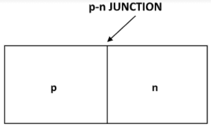
When a p-type semiconductor is suitably joined to an n- type semiconductor, their contact surface is called a p-n junction. The electronic device consisting of a p-n junction is called a p-n junction diode. It has two terminals. One is connected to the p-type crystal and the other is connected to the n-type crystal. It is denoted by the symbol as shown in the figure below. The terminal connected to the p-type crystal may be called as anode and that connected to the n-type crystal may be called as cathode.
When a p-n junction is formed, the electrons diffuse across the junction from n-type to p-type crystal. Similarly, holes diffuse from p-type to n-type crystals. As a result, the n-type crystal acquires a positive potential and the p-type crystal acquires a negative potential. The potential difference created across the p-n junction due to the diffusion of electrons and holes; is called a potential barrier. Then, a thin layer is formed on both the sides of the p-n junction where the mobile charge carriers have been diffused away. This is the depletion layer.
A diode is either forward bias or reverse bias. A p-n junction is said to be forward biased when the external potential difference applied across it is opposite to the potential barrier. And when the external potential difference applied across it is in the same direction as the potential barrier, then it is said to be reverse biased.

Note:
The potential barrier differs from material to material. For example, the potential barrier across a germanium p-n junction is about 0.3V and that across the silicon p-n junction is about 0.7V. This is because of the diffusion of electrons and holes.
When the positive terminal of the source is connected to the P side and the negative terminal is connected to N side then the junction diode is said to be connected in forward bias condition.
Complete step by step answer:
When a p-type semiconductor is suitably joined to an n- type semiconductor, their contact surface is called a p-n junction. The electronic device consisting of a p-n junction is called a p-n junction diode. It has two terminals. One is connected to the p-type crystal and the other is connected to the n-type crystal. It is denoted by the symbol as shown in the figure below. The terminal connected to the p-type crystal may be called as anode and that connected to the n-type crystal may be called as cathode.
When a p-n junction is formed, the electrons diffuse across the junction from n-type to p-type crystal. Similarly, holes diffuse from p-type to n-type crystals. As a result, the n-type crystal acquires a positive potential and the p-type crystal acquires a negative potential. The potential difference created across the p-n junction due to the diffusion of electrons and holes; is called a potential barrier. Then, a thin layer is formed on both the sides of the p-n junction where the mobile charge carriers have been diffused away. This is the depletion layer.
A diode is either forward bias or reverse bias. A p-n junction is said to be forward biased when the external potential difference applied across it is opposite to the potential barrier. And when the external potential difference applied across it is in the same direction as the potential barrier, then it is said to be reverse biased.
Note:
The potential barrier differs from material to material. For example, the potential barrier across a germanium p-n junction is about 0.3V and that across the silicon p-n junction is about 0.7V. This is because of the diffusion of electrons and holes.
When the positive terminal of the source is connected to the P side and the negative terminal is connected to N side then the junction diode is said to be connected in forward bias condition.
Recently Updated Pages
Which of the following graphs shows the variation of class 12 physics CBSE

Draw a labelled diagram of the human male reproductive class 12 biology CBSE
Describe the experiment to compare the emf of two cells class 12 physics CBSE
What is standard hydrogen electrode
What is conventional current and electric current class 12 physics CBSE
2Bromopentane is treated with an alcoholic KOH solution class 12 chemistry CBSE
Trending doubts
Draw a labelled sketch of the human eye class 12 physics CBSE
Which are the Top 10 Largest Countries of the World?
Differentiate between homogeneous and heterogeneous class 12 chemistry CBSE
Draw ray diagrams each showing i myopic eye and ii class 12 physics CBSE
Which is the correct genotypic ratio of mendel dihybrid class 12 biology CBSE
What is the Full Form of PVC, PET, HDPE, LDPE, PP and PS ?