



Explain avalanche breakdown in a diode and Zener breakdown in a Zener diode.
Answer
 Verified
670.5k+ views
Hint: There are two types of breakdowns in p-n junctions. Avalanche breakdown occurs due to the rapid collision of electrons with other atoms. Zener breakdown occurs because of the high electric field. Zener breakdown is the controlled version of Avalanche breakdown in a modified p-n junction.
Complete step by step solution:
Let’s first understand the structure of a p-n junction diode. P-type semiconductor is doped with electron deficient Boron, N-type semiconductor is doped with electron rich Arsenic or Phosphorus. Now, when one part of the intrinsic semiconductor is doped as a p-type material, and the other part is doped with n-type material, it is called a p-n junction diode.
The p-n diode can react to negative potential in two different ways -
(a) Avalanche breakdown
(b) Zener breakdown.
Avalanche Breakdown:
This type of breakdown occurs in the presence of a high electric field. When we apply a high electric field in a reverse biased condition, the electrons start gaining high kinetic energy. These electrons start breaking other covalent bonds and start creating more hole-electron pairs. These pairs start crossing the depletion region and contribute to a high reverse reverse biased current. The breaking of bond is an irreversible process, and the p-n junction is completely destroyed after an avalanche breakdown.
Zener Breakdown:
Zener Breakdown is a controlled way of creating breakdown in p-n junction diodes. The p-n junction has to be heavily doped so that the electrons in the valence bond of p-type region can jump easily to the conduction band of n-type region. This temporary breakdown occurs due to the high electric field. As it does not contribute to a chain reaction, the effects of Zener breakdown is temporary.
You can see the following I-V diagram to understand the two breakdowns.
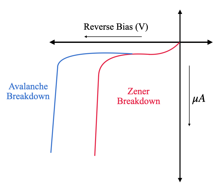
Note: As you can see in the previous diagram, Zener breakdown occurs at a much lesser voltage. Hence, we can use this property in the circuit as a circuit breaker. Wherever the voltage across a Zener diode is above a certain value, it offers a low resistance path for the current flow. A Zener diode can also be used as a voltage regulator.
Complete step by step solution:
Let’s first understand the structure of a p-n junction diode. P-type semiconductor is doped with electron deficient Boron, N-type semiconductor is doped with electron rich Arsenic or Phosphorus. Now, when one part of the intrinsic semiconductor is doped as a p-type material, and the other part is doped with n-type material, it is called a p-n junction diode.
The p-n diode can react to negative potential in two different ways -
(a) Avalanche breakdown
(b) Zener breakdown.
Avalanche Breakdown:
This type of breakdown occurs in the presence of a high electric field. When we apply a high electric field in a reverse biased condition, the electrons start gaining high kinetic energy. These electrons start breaking other covalent bonds and start creating more hole-electron pairs. These pairs start crossing the depletion region and contribute to a high reverse reverse biased current. The breaking of bond is an irreversible process, and the p-n junction is completely destroyed after an avalanche breakdown.
Zener Breakdown:
Zener Breakdown is a controlled way of creating breakdown in p-n junction diodes. The p-n junction has to be heavily doped so that the electrons in the valence bond of p-type region can jump easily to the conduction band of n-type region. This temporary breakdown occurs due to the high electric field. As it does not contribute to a chain reaction, the effects of Zener breakdown is temporary.
You can see the following I-V diagram to understand the two breakdowns.
Note: As you can see in the previous diagram, Zener breakdown occurs at a much lesser voltage. Hence, we can use this property in the circuit as a circuit breaker. Wherever the voltage across a Zener diode is above a certain value, it offers a low resistance path for the current flow. A Zener diode can also be used as a voltage regulator.
Recently Updated Pages
Master Class 12 Physics: Engaging Questions & Answers for Success

Master Class 12 Social Science: Engaging Questions & Answers for Success
Master Class 12 English: Engaging Questions & Answers for Success
Master Class 12 Maths: Engaging Questions & Answers for Success
Master Class 12 Business Studies: Engaging Questions & Answers for Success
Master Class 12 Chemistry: Engaging Questions & Answers for Success
Trending doubts
Draw a labelled sketch of the human eye class 12 physics CBSE
Which are the Top 10 Largest Countries of the World?
Draw ray diagrams each showing i myopic eye and ii class 12 physics CBSE
Which is the correct genotypic ratio of mendel dihybrid class 12 biology CBSE
Which is the strongest oxidising agent out of the following class 12 chemistry CBSE
Differentiate between homogeneous and heterogeneous class 12 chemistry CBSE