


What is the depletion region in p-n junction?
Answer
617.4k+ views
Hint: A p-n junction is a boundary between p and n-type of semiconductors. A p-n junction is formed by doping one portion of a p-type semiconductor with a pentavalent impurity. During the formation of the p-n junction, a region at p-n junction acts as the barrier and stops any flow of electrons from the n region to the p region.
Complete step-by-step solution:
A p-n junction is the basic block of many semiconductor devices like diodes, transistors, etc. A p-n junction is formed by converting a part of a p-type semiconductor to n-type.
During the formation of the p-n junction, two processes occur: Diffusion and drift.
In an n-type semiconductor, the concentration of electrons is more compared to the concentration of holes. Similarly, in a p-type semiconductor, the concentration of holes is more than the concentration of electrons. During the formation of the p-n junction, due to the concentration difference across p-, and n- sides, holes diffuse from p-side to n-side, and electrons diffuse from the n-side to the p-side which gives rise to diffusion current across the junction.
When an electron diffuses from n to “p”, it leaves behind a positive charge on the n-side. This positive charge is immobile as it is bonded to the surrounding atoms. As the electrons continue to diffuse from n to “p”, a layer of positive charge on the n-side of the junction is developed.
When a hole diffuses from p to n due to the concentration difference, it leaves behind a negative charge which is immobile. As the holes continue to diffuse, a layer of negative charge (or negative space-charge region) on the p-side of the junction is developed. This space-charge region on either side of the junction together is known as the depletion region as the electrons and holes taking part in the initial movement across the junction depleted the region of its free charges.
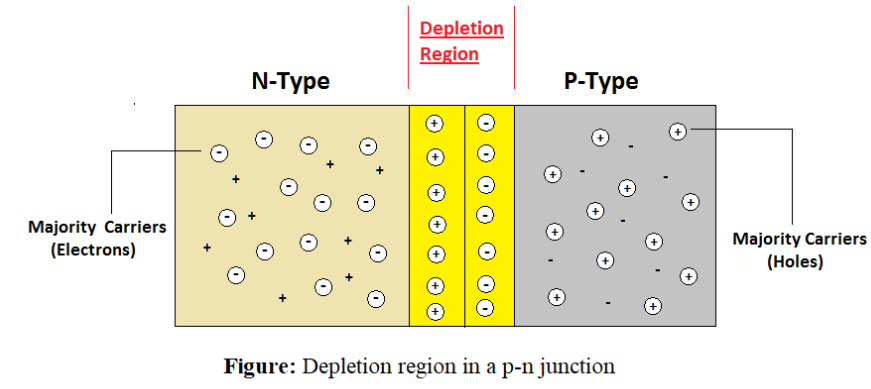
Note: The thickness of the depletion region is very small and is of the order of one-tenth of a micrometer. Due to the positive space-charge region on the n-side of the junction and negative space charge region on the p-side of the junction, an electric field directed from positive charge to negative charge develops. Due to this field, an electron on the p-side of the junction moves to the n-side, and a hole on the n-side of the junction moves to the p-side. The motion of electrons and holes due to the electric field is called drift.
Complete step-by-step solution:
A p-n junction is the basic block of many semiconductor devices like diodes, transistors, etc. A p-n junction is formed by converting a part of a p-type semiconductor to n-type.
During the formation of the p-n junction, two processes occur: Diffusion and drift.
In an n-type semiconductor, the concentration of electrons is more compared to the concentration of holes. Similarly, in a p-type semiconductor, the concentration of holes is more than the concentration of electrons. During the formation of the p-n junction, due to the concentration difference across p-, and n- sides, holes diffuse from p-side to n-side, and electrons diffuse from the n-side to the p-side which gives rise to diffusion current across the junction.
When an electron diffuses from n to “p”, it leaves behind a positive charge on the n-side. This positive charge is immobile as it is bonded to the surrounding atoms. As the electrons continue to diffuse from n to “p”, a layer of positive charge on the n-side of the junction is developed.
When a hole diffuses from p to n due to the concentration difference, it leaves behind a negative charge which is immobile. As the holes continue to diffuse, a layer of negative charge (or negative space-charge region) on the p-side of the junction is developed. This space-charge region on either side of the junction together is known as the depletion region as the electrons and holes taking part in the initial movement across the junction depleted the region of its free charges.
Note: The thickness of the depletion region is very small and is of the order of one-tenth of a micrometer. Due to the positive space-charge region on the n-side of the junction and negative space charge region on the p-side of the junction, an electric field directed from positive charge to negative charge develops. Due to this field, an electron on the p-side of the junction moves to the n-side, and a hole on the n-side of the junction moves to the p-side. The motion of electrons and holes due to the electric field is called drift.
Recently Updated Pages
Master Class 12 Economics: Engaging Questions & Answers for Success
Master Class 12 English: Engaging Questions & Answers for Success
Master Class 12 Social Science: Engaging Questions & Answers for Success
Master Class 12 Maths: Engaging Questions & Answers for Success
Master Class 12 Physics: Engaging Questions & Answers for Success
Master Class 12 Business Studies: Engaging Questions & Answers for Success
Trending doubts
Which are the Top 10 Largest Countries of the World?
Draw a labelled sketch of the human eye class 12 physics CBSE
Differentiate between homogeneous and heterogeneous class 12 chemistry CBSE
Why is the cell called the structural and functional class 12 biology CBSE
Draw ray diagrams each showing i myopic eye and ii class 12 physics CBSE
Which is the correct genotypic ratio of mendel dihybrid class 12 biology CBSE