


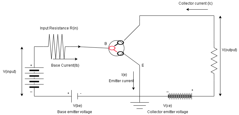
Define common-emitter output characteristics for a transistor. Draw a circuit diagram for studying the characteristics of an n-p-n transistor in common emitter configuration.
Among emitter, base, and collector regions of a transistor which one is:
a) Largest in size
b) Most heavily doped?
Answer
642.9k+ views
Hint: A transistor is a semiconductor device that has three terminals and it is used to amplify or switch the electronic signals. It transfers a weak signal from a low resistance circuit to high resistance.
Complete step by step solution:
Step I:
The configuration of a transistor in which the emitter is connected between collector and base is known as common emitter configuration. In this configuration, the input circuit consists of emitter and base while the output circuit is connected between collector and emitter.
Step II:
NPN transistor is Bipolar Junction Transistor. This transistor has three terminals – emitter, base, and collector. It consists of two n-type semiconductor materials and one p-type semiconductor material in between two n-type semiconductors. It is the most used type of transistors because in this the electrons have higher mobility or flowing rate than holes. Due to the movement of the electrons from emitter to collector, the current flows in the circuit.
Step III:
The collector has the largest regions among emitter, base, and collector. This is because the electrons moving from emitter to collector junction will collect here. It is given a large area because it provides a large area for the heat to be generated and will not result in a rise in temperature in the transistor.
The emitter in the transistor is heavily doped. It is because the function of the emitter is to provide or inject electrons and holes to the base. Heavy doping helps in the greater supply of charge carriers and hence the output current in the circuit also increases.
The collector has the largest regions among emitter, base, and collector. The emitter in the transistor is heavily doped.
Note:
In the n-p-n transistor, the emitter is heavily doped but the collector is moderately doped. This is because if the collector is also heavily doped then the electrons coming from the emitter and base junction will suffer a repulsion and will not be able to accumulate. The net flow of current in the circuit can decrease.
Recently Updated Pages
Basicity of sulphurous acid and sulphuric acid are
Master Class 12 Economics: Engaging Questions & Answers for Success
Master Class 12 Biology: Engaging Questions & Answers for Success
Master Class 11 English: Engaging Questions & Answers for Success
Master Class 11 Physics: Engaging Questions & Answers for Success
Master Class 11 Computer Science: Engaging Questions & Answers for Success
Trending doubts
Draw a labelled sketch of the human eye class 12 physics CBSE
The chemical formula of tear gas is A CO Cl 2 B C 10 class 12 chemistry CBSE
Draw ray diagrams each showing i myopic eye and ii class 12 physics CBSE
Which are the Top 10 Largest Countries of the World?
Differentiate between homogeneous and heterogeneous class 12 chemistry CBSE
Which is the correct genotypic ratio of mendel dihybrid class 12 biology CBSE