


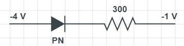
What is the current in the circuit shown below?
$\begin{align}
& \left( \text{A} \right)\text{ 0A} \\
& \left( \text{B} \right)\text{ 1}{{\text{0}}^{-2}}A \\
& \left( \text{C} \right)\text{ 1A} \\
& \left( \text{D} \right)\text{ 0}\text{.10A} \\
\end{align}$
Answer
641.1k+ views
Hint: We have provided a figure, in which N side of diode is correct to higher potential which P side to lower potential. When the n-region of PN diode connects to a positive terminal of source and vice-versa then p-n junction width increases and leads to go under reverse biased region.
Complete step by step answer:
Complete step by step answer:

We know that, when P and N regions of the diode are connected to the positive & negative terminal of an external source like battery then the diode is said to be connected in reverse bias.
As you can see in the figure, the diode has two terminals, namely positive and negative. Positive is known as P region i.e. region of holes and negative is known as n-region i.e. region of electrons.
As shown in figure, positive terminal of PN diode is connected to less value of voltage i.e. -4V and the negative terminal of the PN diode is connected to high voltage. It is called a high voltage because -1 is greater than -4. Above statement means that the diode is in reversed biased condition.
The holes of the P-side are attracted towards negative termination of external source and electrons are pulled towards the positive terminal which acts as majority carriers. Thus both holes and electrons move away from the junction. Therefore, it causes an increase in depution region and potential barrier. As there is no crossing of majority carriers across the junction, there is no flow of current through the circuit as well as diode (junction).
According to above theory, in reverse biased condition no current flows, i.e. zero ampere. Therefore, the correct option is (A).
Note:
Students consider that not at all current flow in circuit but this is not case, a small amount of current still flows through circuit. But it is not that effective. Therefore it can be neglected. In reverse biased condition, a diode or circuit or P-N junction acts as an insulator which prevents the flow of current. Small or negligible current flows through the circuit because of thermally produced minority carriers in depletion regions. It acts as an open switch and not at all current flows through it.
Complete step by step answer:
Complete step by step answer:
We know that, when P and N regions of the diode are connected to the positive & negative terminal of an external source like battery then the diode is said to be connected in reverse bias.
As you can see in the figure, the diode has two terminals, namely positive and negative. Positive is known as P region i.e. region of holes and negative is known as n-region i.e. region of electrons.
As shown in figure, positive terminal of PN diode is connected to less value of voltage i.e. -4V and the negative terminal of the PN diode is connected to high voltage. It is called a high voltage because -1 is greater than -4. Above statement means that the diode is in reversed biased condition.
The holes of the P-side are attracted towards negative termination of external source and electrons are pulled towards the positive terminal which acts as majority carriers. Thus both holes and electrons move away from the junction. Therefore, it causes an increase in depution region and potential barrier. As there is no crossing of majority carriers across the junction, there is no flow of current through the circuit as well as diode (junction).
According to above theory, in reverse biased condition no current flows, i.e. zero ampere. Therefore, the correct option is (A).
Note:
Students consider that not at all current flow in circuit but this is not case, a small amount of current still flows through circuit. But it is not that effective. Therefore it can be neglected. In reverse biased condition, a diode or circuit or P-N junction acts as an insulator which prevents the flow of current. Small or negligible current flows through the circuit because of thermally produced minority carriers in depletion regions. It acts as an open switch and not at all current flows through it.
Recently Updated Pages
Basicity of sulphurous acid and sulphuric acid are
Master Class 12 Economics: Engaging Questions & Answers for Success
Master Class 12 Biology: Engaging Questions & Answers for Success
Master Class 11 English: Engaging Questions & Answers for Success
Master Class 11 Physics: Engaging Questions & Answers for Success
Master Class 11 Computer Science: Engaging Questions & Answers for Success
Trending doubts
Draw a labelled sketch of the human eye class 12 physics CBSE
The chemical formula of tear gas is A CO Cl 2 B C 10 class 12 chemistry CBSE
Draw ray diagrams each showing i myopic eye and ii class 12 physics CBSE
Which are the Top 10 Largest Countries of the World?
Differentiate between homogeneous and heterogeneous class 12 chemistry CBSE
Which is the correct genotypic ratio of mendel dihybrid class 12 biology CBSE