


What causes the depletion region ?
Answer
546.3k+ views
Hint: In order to understand depletion region, we need to understand about the PN junction. PN junction diode is a combination of two types of semiconductor one is of P-type which contains excess amount of holes and other is N-type which contain excess amount of electrons. Both layers of P-type and N-type are joined together and form a P-N junction Diode.
Complete answer:
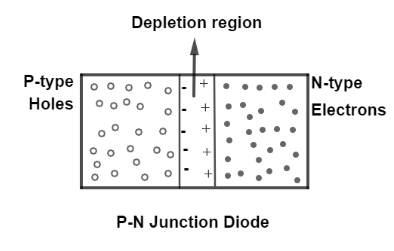
As soon as the P-N junction diode is formed , the holes in P-type regions starts to diffuse in to N-side of the junction and when this hole which has a positive charge move to the N-type of junction it leaves the space near the junction creating negative charge and similarly when the electrons which have a negative charge starts to diffuse towards the P-type part of junction diode, as soon as electron enter in P-type part of diode, electron leaves the space near the junction creating positive charge.
This space near the junction carrying those positive and negative charges is known as depletion region or depletion layer.Hence, the diffusion of holes and electrons in N-type region and P-type regions to neutralize the both regions of the PN junction is the cause of depletion region formation.
Depletion region is shown in the diagram below as:
Note: It should be remembered that, when a PN junction diode is connected in forward bias then the width of depletion regions gets decreased whereas in case of backward bias, the width of depletion region gets increased. Forward bias means when P-type of junction is connected to Positive terminal of battery and backward bias is when P-type is connected to negative terminal of the battery.
Complete answer:
As soon as the P-N junction diode is formed , the holes in P-type regions starts to diffuse in to N-side of the junction and when this hole which has a positive charge move to the N-type of junction it leaves the space near the junction creating negative charge and similarly when the electrons which have a negative charge starts to diffuse towards the P-type part of junction diode, as soon as electron enter in P-type part of diode, electron leaves the space near the junction creating positive charge.
This space near the junction carrying those positive and negative charges is known as depletion region or depletion layer.Hence, the diffusion of holes and electrons in N-type region and P-type regions to neutralize the both regions of the PN junction is the cause of depletion region formation.
Depletion region is shown in the diagram below as:
Note: It should be remembered that, when a PN junction diode is connected in forward bias then the width of depletion regions gets decreased whereas in case of backward bias, the width of depletion region gets increased. Forward bias means when P-type of junction is connected to Positive terminal of battery and backward bias is when P-type is connected to negative terminal of the battery.
Recently Updated Pages
Master Class 12 Business Studies: Engaging Questions & Answers for Success
Master Class 12 Chemistry: Engaging Questions & Answers for Success
Master Class 12 Biology: Engaging Questions & Answers for Success
Class 12 Question and Answer - Your Ultimate Solutions Guide
Master Class 11 English: Engaging Questions & Answers for Success
Master Class 11 Social Science: Engaging Questions & Answers for Success
Trending doubts
Which are the Top 10 Largest Countries of the World?
Draw a labelled sketch of the human eye class 12 physics CBSE
The end of compass needle which points towards north class 12 physics CBSE
Differentiate between homogeneous and heterogeneous class 12 chemistry CBSE
In order to find out the different types of gametes class 12 biology NEET_UG
Why is the cell called the structural and functional class 12 biology CBSE