


Are LEDs reverse biased?
Answer
573.3k+ views
Hint: Recall that LEDS are basically diodes that emit light. We know that electrons emit light when they deexcite from the conduction band to the valence band following which they recombine with the holes in the valence band. In such a case, determine in which configuration of the LED such recombination of charge carriers occurs. This will be the operational configuration of the LED. Remember that the LED is reverse biased when the p-side and the n-side are connected to the negative and positive terminals of a battery respectively.
Complete answer:
We know that a Light Emitting Diode (LED) is a semiconducting device that emits light. It is a diode and consists of three regions: p-region, the n-region and the depletion region as shown in the diagram.
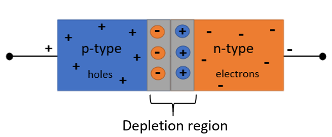
The p-region consists of free holes and the n-region consists of free electrons whereas the depletion region between them consists of immobile charge carriers. This region acts as a barrier to the electric current. When a suitable voltage greater than the barrier potential is applied, electric current starts flowing through the diode.
When the LED is forward biased (i.e., when the p-side and the n-side are connected to the positive and negative terminals of a battery respectively), the free electrons in the n-region and the holes in the p-region get attracted towards the opposite ends and are pushed towards the junction or the depletion region. When free electrons from the n-side reach the junction, they recombine with the holes in the depletion region and when holes from the p-side reach the junction, they recombine with the electrons in the depletion region. Because of the recombination of free electrons and holes in the depletion region, the width of the depletion region decreases, as a result of which more charge carriers are able to cross the p-n junction. This recombination of free electrons in the conduction band with the holes in the valence band occurs when the free electrons lose energy in the form of light and fall back to the valence band and recombine with the holes. Each recombination will emit some light energy, making the diode glow, and the intensity of the emitted light is proportional to the energy gap between the conduction and valence bands.
When the LED is reverse biased, (i.e., when the p-side and the n-side are connected to the negative and positive terminals of a battery respectively), the free electrons in the n-region and the holes in the p-region get repelled away from the junction towards their periphery and as a result, the width of the depletion layer increases and no recombination of charge carriers occurs, due to which it emits no light. However, if the LED is supplied a higher (breakdown) voltage in this configuration, it begins to conduct electric current and gets irreversibly damaged.
Thus, LEDs are operated in the forward biased condition where they are able to undergo recombination of charge carriers to subsequently emit light of suitable wavelength.
Note:
It is important to understand how the depletion region is formed in the first place. We know that a p-n junction diode is formed when positive p-type (hole-rich) and negative n-type (electron-rich) semiconductors are joined, resulting in an interface between them called the p-n junction. This junction is formed by the diffusion of holes from the p-side to the n-side, and the diffusion of electrons from the n-side to the p-side due to a difference in concentration. A layer of positive charge or holes is developed on the n-side and a layer of negative charge or electrons is developed on the p-side. These two layers together are called the depletion layer.
Remember that in the band structure of the n and p-type semiconductors the electrons in the conduction band and the holes in the valence band are the majority charge carriers respectively.
Complete answer:
We know that a Light Emitting Diode (LED) is a semiconducting device that emits light. It is a diode and consists of three regions: p-region, the n-region and the depletion region as shown in the diagram.
The p-region consists of free holes and the n-region consists of free electrons whereas the depletion region between them consists of immobile charge carriers. This region acts as a barrier to the electric current. When a suitable voltage greater than the barrier potential is applied, electric current starts flowing through the diode.
When the LED is forward biased (i.e., when the p-side and the n-side are connected to the positive and negative terminals of a battery respectively), the free electrons in the n-region and the holes in the p-region get attracted towards the opposite ends and are pushed towards the junction or the depletion region. When free electrons from the n-side reach the junction, they recombine with the holes in the depletion region and when holes from the p-side reach the junction, they recombine with the electrons in the depletion region. Because of the recombination of free electrons and holes in the depletion region, the width of the depletion region decreases, as a result of which more charge carriers are able to cross the p-n junction. This recombination of free electrons in the conduction band with the holes in the valence band occurs when the free electrons lose energy in the form of light and fall back to the valence band and recombine with the holes. Each recombination will emit some light energy, making the diode glow, and the intensity of the emitted light is proportional to the energy gap between the conduction and valence bands.
When the LED is reverse biased, (i.e., when the p-side and the n-side are connected to the negative and positive terminals of a battery respectively), the free electrons in the n-region and the holes in the p-region get repelled away from the junction towards their periphery and as a result, the width of the depletion layer increases and no recombination of charge carriers occurs, due to which it emits no light. However, if the LED is supplied a higher (breakdown) voltage in this configuration, it begins to conduct electric current and gets irreversibly damaged.
Thus, LEDs are operated in the forward biased condition where they are able to undergo recombination of charge carriers to subsequently emit light of suitable wavelength.
Note:
It is important to understand how the depletion region is formed in the first place. We know that a p-n junction diode is formed when positive p-type (hole-rich) and negative n-type (electron-rich) semiconductors are joined, resulting in an interface between them called the p-n junction. This junction is formed by the diffusion of holes from the p-side to the n-side, and the diffusion of electrons from the n-side to the p-side due to a difference in concentration. A layer of positive charge or holes is developed on the n-side and a layer of negative charge or electrons is developed on the p-side. These two layers together are called the depletion layer.
Remember that in the band structure of the n and p-type semiconductors the electrons in the conduction band and the holes in the valence band are the majority charge carriers respectively.
Recently Updated Pages
Master Class 12 Economics: Engaging Questions & Answers for Success
Master Class 12 English: Engaging Questions & Answers for Success
Master Class 12 Social Science: Engaging Questions & Answers for Success
Master Class 12 Maths: Engaging Questions & Answers for Success
Master Class 12 Physics: Engaging Questions & Answers for Success
Master Class 9 General Knowledge: Engaging Questions & Answers for Success
Trending doubts
Which are the Top 10 Largest Countries of the World?
Draw a labelled sketch of the human eye class 12 physics CBSE
Differentiate between homogeneous and heterogeneous class 12 chemistry CBSE
Why is the cell called the structural and functional class 12 biology CBSE
Draw ray diagrams each showing i myopic eye and ii class 12 physics CBSE
Which is the correct genotypic ratio of mendel dihybrid class 12 biology CBSE