


A transistor is used in common-emitter mode in an amplifier circuit. When a signal of $20mV$ is added to the base-emitter voltage, the base current changes by $20\mu A$ and the collector current changes by $2mA$. The load resistance is $5k\Omega $. Calculate (a) the factor $\beta$, (b) the input resistance ${{R}_{BE}}$, (c) the trans conductance and (d) the voltage gain.
Answer
590.1k+ views
Hint: Emitter current for a common emitter configuration is defined as ${{I}_{E}}={{I}_{C}}+{{I}_{B}}$, and the current gain is the ratio of ${{I}_{C}}$ and ${{I}_{B}}$.
Use Kirchoff’s voltage law to obtain expression for required quantity.
In a transistor, current gain is defined as the factor by which current is amplified in the circuit. Current gain is denoted by $\beta$.
The trans conductance of a CE configured transistor is defined as ratio of collector current to the base emitter input voltage.
Voltage gain is defined as the factor by which input voltage is amplified.
Formula used:
$\beta =\dfrac{\Delta {{I}_{C}}}{\Delta {{I}_{B}}}$
Complete step-by-step answer:
In the Common Emitter configuration, the input signal is applied between the base and the emitter, and the output is taken from between the collector and the emitter as shown. Common emitter type of configuration is the most commonly used for transistor based amplifiers.
In common emitter configuration of bipolar junction transistor, the current flowing out of the transistor must be equal to the currents flowing into the transistor as the emitter current is given as
${{I}_{E}}={{I}_{C}}+{{I}_{B}}$
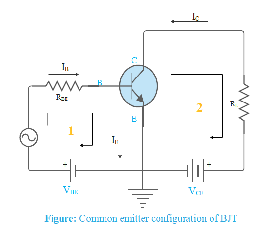
Load resistance ${{R}_{L}}$ is connected in series with the collector. The current gain of the common emitter transistor configuration is written as
$\beta =\dfrac{{{I}_{C}}}{{{I}_{B}}}$
In this question, ${{I}_{C}}$ is $2mA$ and ${{I}_{B}}=20\mu A$
Therefore, $\beta =\dfrac{2m}{20\mu }=\dfrac{2\times {{10}^{-3}}}{20\times {{10}^{-6}}}=100$
Applying Kirchoff’s law in loop 1, we get
$-{{V}_{BE}}+{{I}_{B}}{{R}_{BE}}=0$
$\Rightarrow {{R}_{BE}}=\dfrac{{{V}_{BE}}}{{{I}_{B}}}=\dfrac{20mV}{20\mu A}={{10}^{3}}\Omega $
${{R}_{BE}}=1k\Omega $
Trans conductance of a CE amplifier is the ratio of current gain to the voltage applied. Therefore,
Trans conductance = $\dfrac{{{I}_{C}}}{{{V}_{BE}}}=\dfrac{2mA}{20mV}=0.1mho$
The change in output voltage can be calculated by applying Kirchoff’s voltage law in loop 2
$-{{V}_{CE}}+{{I}_{C}}{{R}_{L}}=0$
$\Rightarrow {{V}_{CE}}={{I}_{C}}{{R}_{L}}=2mA\times 5k\Omega =10V$
Applied signal voltage is, ${{V}_{in}}=20mV$
Voltage gain = $\dfrac{{{V}_{out}}}{{{V}_{in}}}=\dfrac{{{V}_{CE}}}{{{V}_{BE}}}=\dfrac{10V}{20mV}=500$
Note: Common emitter configuration of bipolar junction transistor has a greater input impedance, current and power gain than that of the common base configuration but its voltage gain is much lower. The common emitter configuration acts as an inverting amplifier circuit. This implies that the resulting output signal has a ${{180}^{{}^\circ }}$ phase-shift with regards to the input voltage signal.
Use Kirchoff’s voltage law to obtain expression for required quantity.
In a transistor, current gain is defined as the factor by which current is amplified in the circuit. Current gain is denoted by $\beta$.
The trans conductance of a CE configured transistor is defined as ratio of collector current to the base emitter input voltage.
Voltage gain is defined as the factor by which input voltage is amplified.
Formula used:
$\beta =\dfrac{\Delta {{I}_{C}}}{\Delta {{I}_{B}}}$
Complete step-by-step answer:
In the Common Emitter configuration, the input signal is applied between the base and the emitter, and the output is taken from between the collector and the emitter as shown. Common emitter type of configuration is the most commonly used for transistor based amplifiers.
In common emitter configuration of bipolar junction transistor, the current flowing out of the transistor must be equal to the currents flowing into the transistor as the emitter current is given as
${{I}_{E}}={{I}_{C}}+{{I}_{B}}$
Load resistance ${{R}_{L}}$ is connected in series with the collector. The current gain of the common emitter transistor configuration is written as
$\beta =\dfrac{{{I}_{C}}}{{{I}_{B}}}$
In this question, ${{I}_{C}}$ is $2mA$ and ${{I}_{B}}=20\mu A$
Therefore, $\beta =\dfrac{2m}{20\mu }=\dfrac{2\times {{10}^{-3}}}{20\times {{10}^{-6}}}=100$
Applying Kirchoff’s law in loop 1, we get
$-{{V}_{BE}}+{{I}_{B}}{{R}_{BE}}=0$
$\Rightarrow {{R}_{BE}}=\dfrac{{{V}_{BE}}}{{{I}_{B}}}=\dfrac{20mV}{20\mu A}={{10}^{3}}\Omega $
${{R}_{BE}}=1k\Omega $
Trans conductance of a CE amplifier is the ratio of current gain to the voltage applied. Therefore,
Trans conductance = $\dfrac{{{I}_{C}}}{{{V}_{BE}}}=\dfrac{2mA}{20mV}=0.1mho$
The change in output voltage can be calculated by applying Kirchoff’s voltage law in loop 2
$-{{V}_{CE}}+{{I}_{C}}{{R}_{L}}=0$
$\Rightarrow {{V}_{CE}}={{I}_{C}}{{R}_{L}}=2mA\times 5k\Omega =10V$
Applied signal voltage is, ${{V}_{in}}=20mV$
Voltage gain = $\dfrac{{{V}_{out}}}{{{V}_{in}}}=\dfrac{{{V}_{CE}}}{{{V}_{BE}}}=\dfrac{10V}{20mV}=500$
Note: Common emitter configuration of bipolar junction transistor has a greater input impedance, current and power gain than that of the common base configuration but its voltage gain is much lower. The common emitter configuration acts as an inverting amplifier circuit. This implies that the resulting output signal has a ${{180}^{{}^\circ }}$ phase-shift with regards to the input voltage signal.
Recently Updated Pages
Basicity of sulphurous acid and sulphuric acid are
Master Class 12 English: Engaging Questions & Answers for Success
Master Class 12 Social Science: Engaging Questions & Answers for Success
Master Class 12 Maths: Engaging Questions & Answers for Success
Master Class 12 Economics: Engaging Questions & Answers for Success
Master Class 12 Physics: Engaging Questions & Answers for Success
Trending doubts
Give 10 examples of unisexual and bisexual flowers
Coming together federation is practiced in A India class 12 social science CBSE
Write the formula to find the shortest distance between class 12 maths CBSE
Find the foot of the perpendicular from point232to class 12 maths CBSE
How was the Civil Disobedience Movement different from class 12 social science CBSE
How is democracy better than other forms of government class 12 social science CBSE