


Draw a circuit diagram of a transistor amplifier in CE configuration.
Define the terms:
(i) Input resistance and
(ii) Current amplification factor.
How are these determined using typical input and output characteristics?
Answer
596.1k+ views
Hint: Recall the common emitter configuration of a transistor amplifier. Also recall its circuit diagram, its V-I characteristics graph. Always remember, in common emitter configuration, the input current and the output voltage are taken as the independent variables, whereas the input voltage and output current are the dependent variables.
Complete step by step solution:
The circuit diagram of a transistor amplifier in Common-Emitter configuration is given by,
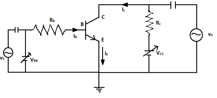
(i) Input resistance :- It is defined as the ratio of change in base-emitter voltage to the change in base current at constant ${V_{CE}}$ . The change in base-emitter voltage that is $\Delta {V_{BE}}$ and the change in base current that is $\Delta {I_B}$ can be calculated from the input characteristics of the transistor amplifier in CE configuration.
Mathematically, Input resistance is defined by,
${R_{iB}} = \left( {\dfrac{{\Delta {V_{BE}}}}{{\Delta {I_B}}}} \right)$ at constant ${V_{CE}}$
Where, $\Delta {V_{BE}}$ is the change in base-emitter voltage
$\Delta {I_B}$ is the change in the base current
${V_{CE}}$ is the collector-emitter voltage
For finding the input resistance, we have to mark a point P on the input characteristics and then draw a tangent at point P and then the reciprocal of slope AB will give us the input resistance.
(ii) Current amplification factor :- It is defined as the ratio of the change in collector current to the change in the base current taking collector voltage constant. It is denoted by $\beta $
Mathematically, current amplification factor is defined by,
$\beta = \left( {\dfrac{{\Delta {I_C}}}{{\Delta {I_B}}}} \right)$ at constant $V_{CB}$.
Where, \[\Delta {I_C}\] is the change in collector current.
$\Delta {I_B}$ is the change in the base current.
The value of current amplification factor is obtained from the Output characteristic graph that is $I_C$ versus $V_{CE}$ plot by using different values of $I_B$.
Note: The common-emitter configuration provides good current gain and voltage gain. As the input resistance is of very low value, a small value of $\Delta {V_{BE}}$ is enough to produce a large current flow of the base current. The current gain in Common Emitter connection is very high. This is the reason this circuit connection is mostly used in all transistor applications.
Complete step by step solution:
The circuit diagram of a transistor amplifier in Common-Emitter configuration is given by,
(i) Input resistance :- It is defined as the ratio of change in base-emitter voltage to the change in base current at constant ${V_{CE}}$ . The change in base-emitter voltage that is $\Delta {V_{BE}}$ and the change in base current that is $\Delta {I_B}$ can be calculated from the input characteristics of the transistor amplifier in CE configuration.
Mathematically, Input resistance is defined by,
${R_{iB}} = \left( {\dfrac{{\Delta {V_{BE}}}}{{\Delta {I_B}}}} \right)$ at constant ${V_{CE}}$
Where, $\Delta {V_{BE}}$ is the change in base-emitter voltage
$\Delta {I_B}$ is the change in the base current
${V_{CE}}$ is the collector-emitter voltage
For finding the input resistance, we have to mark a point P on the input characteristics and then draw a tangent at point P and then the reciprocal of slope AB will give us the input resistance.
(ii) Current amplification factor :- It is defined as the ratio of the change in collector current to the change in the base current taking collector voltage constant. It is denoted by $\beta $
Mathematically, current amplification factor is defined by,
$\beta = \left( {\dfrac{{\Delta {I_C}}}{{\Delta {I_B}}}} \right)$ at constant $V_{CB}$.
Where, \[\Delta {I_C}\] is the change in collector current.
$\Delta {I_B}$ is the change in the base current.
The value of current amplification factor is obtained from the Output characteristic graph that is $I_C$ versus $V_{CE}$ plot by using different values of $I_B$.
Note: The common-emitter configuration provides good current gain and voltage gain. As the input resistance is of very low value, a small value of $\Delta {V_{BE}}$ is enough to produce a large current flow of the base current. The current gain in Common Emitter connection is very high. This is the reason this circuit connection is mostly used in all transistor applications.
Recently Updated Pages
Master Class 12 Social Science: Engaging Questions & Answers for Success
Master Class 12 Physics: Engaging Questions & Answers for Success
Master Class 12 Maths: Engaging Questions & Answers for Success
Master Class 12 Economics: Engaging Questions & Answers for Success
Master Class 12 Chemistry: Engaging Questions & Answers for Success
Master Class 12 Business Studies: Engaging Questions & Answers for Success
Trending doubts
Which are the Top 10 Largest Countries of the World?
Draw a labelled sketch of the human eye class 12 physics CBSE
Explain the structure of megasporangium class 12 biology CBSE
What are the major means of transport Explain each class 12 social science CBSE
How many chromosomes are found in human ovum a 46 b class 12 biology CBSE
The diagram of the section of a maize grain is given class 12 biology CBSE