


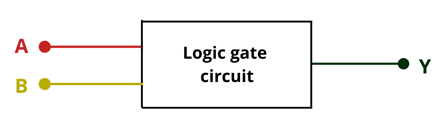
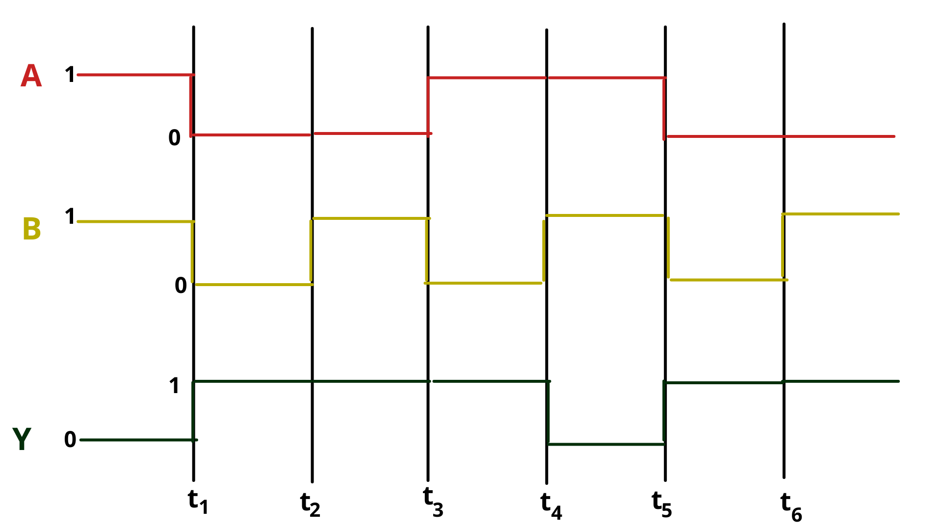
Two following figures show a logic gate circuit with two inputs A and B and the output Y. The voltage waveforms of A, B and Y are as given.
The logic gate is
A. NOR gate
B. OR gate
C. AND gate
D. NAND gate
Answer
562.2k+ views
Hint: In this problem two inputs are given and one output is given in the form of a voltage wave. Based on the input and output values we need to find the logic gate circuit. Draw the truth table for the given six intervals and compare it with the truth tables of NOR gate, OR gate, AND gate and NAND gate.
Complete step by step answer:
Let us draw the truth table for the given circuit. At time interval ${t_1}$ the input is $(1,1)$ and the output is $Y = 0$. Similarly, at time interval \[{t_2}\] the input is \[(0,0)\] and the output is \[Y = 1\].
At \[{t_3}\] input is \[(0,1)\] and the output is \[Y = 1\]
At \[{t_4}\] input is \[(1,0)\] and the output is \[Y = 1\]
At \[{t_5}\] input is $(1,1)$ and output is $Y = 0$.
Using this information, the truth table will be as follows:
The truth tables for NOR, OR, AND and NAND gates are given below:
Truth table for NOR gate:
Truth table for OR gate:
Truth table for AND gate:
Truth table for NAND gate:
The truth table for the given logical gate circuit is the same as the truth table for NAND gate. Therefore, the logic gate is a NAND gate.
So, the correct answer is Option (D).
Note: NAND gate is a combination of AND gate and NOT gate. In AND gate the output is $1$ when the at least one input is $0$ as the output for $0$ input will be zero and NOT for zero is $1$ .NAND gate forms the basis of most practical gates. For NAND gate the output is $0$ when both the inputs are $1$.
Complete step by step answer:
Let us draw the truth table for the given circuit. At time interval ${t_1}$ the input is $(1,1)$ and the output is $Y = 0$. Similarly, at time interval \[{t_2}\] the input is \[(0,0)\] and the output is \[Y = 1\].
At \[{t_3}\] input is \[(0,1)\] and the output is \[Y = 1\]
At \[{t_4}\] input is \[(1,0)\] and the output is \[Y = 1\]
At \[{t_5}\] input is $(1,1)$ and output is $Y = 0$.
Using this information, the truth table will be as follows:
| A | B | Y |
| $1$ | $1$ | $0$ |
| $0$ | $0$ | $1$ |
| $0$ | $1$ | $1$ |
| $1$ | $0$ | $1$ |
| $1$ | $1$ | $0$ |
The truth tables for NOR, OR, AND and NAND gates are given below:
Truth table for NOR gate:
| Input A | Input B | Output |
| $0$ | $0$ | $1$ |
| $0$ | $1$ | $0$ |
| $1$ | $0$ | $0$ |
| $1$ | $1$ | $0$ |
Truth table for OR gate:
| Input A | Input B | Output |
| $0$ | $0$ | $0$ |
| $0$ | $1$ | $1$ |
| $1$ | $0$ | $1$ |
| $1$ | $1$ | $1$ |
Truth table for AND gate:
| Input A | Input B | Output |
| $0$ | $0$ | $0$ |
| $0$ | $1$ | $0$ |
| $1$ | $0$ | $0$ |
| $1$ | $1$ | $1$ |
Truth table for NAND gate:
| Input A | Input B | Output |
| $0$ | $0$ | $1$ |
| $0$ | $1$ | $1$ |
| $1$ | $0$ | $1$ |
| $1$ | $1$ | $0$ |
The truth table for the given logical gate circuit is the same as the truth table for NAND gate. Therefore, the logic gate is a NAND gate.
So, the correct answer is Option (D).
Note: NAND gate is a combination of AND gate and NOT gate. In AND gate the output is $1$ when the at least one input is $0$ as the output for $0$ input will be zero and NOT for zero is $1$ .NAND gate forms the basis of most practical gates. For NAND gate the output is $0$ when both the inputs are $1$.
Recently Updated Pages
Master Class 12 Business Studies: Engaging Questions & Answers for Success
Master Class 12 Chemistry: Engaging Questions & Answers for Success
Master Class 12 Biology: Engaging Questions & Answers for Success
Class 12 Question and Answer - Your Ultimate Solutions Guide
Master Class 11 English: Engaging Questions & Answers for Success
Master Class 11 Maths: Engaging Questions & Answers for Success
Trending doubts
Which is more stable and why class 12 chemistry CBSE
Which are the Top 10 Largest Countries of the World?
Draw a labelled sketch of the human eye class 12 physics CBSE
Differentiate between homogeneous and heterogeneous class 12 chemistry CBSE
What are the major means of transport Explain each class 12 social science CBSE
Sulphuric acid is known as the king of acids State class 12 chemistry CBSE