


Explain with the help of diagram, how a depletion layer and barrier potential are formed in a junction diode.
Answer
595.8k+ views
Hint:There are two types of semiconductors: p-type and n-type. When both p-type and n-type semiconductor fused together, a region of a certain width develops between them. Recall the term barrier potential which is the potential beyond that the depletion region breaks down.
Complete answer:
We know that there are two types of semiconductors: p-type and n-type. When both p-type and n-type semiconductor fused together, a depletion region develops between them. The word depletion meant reduction in something. We know that in p-type semiconductor, holes are majority charge carriers and in n-type semiconductor, electrons are majority charge carriers. The depletion region or pn junction separates p-region and n-region in the semiconductor device.
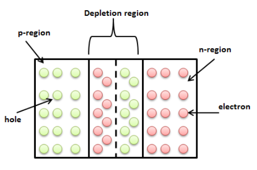
We will now discuss how the depletion region forms? Since in n-type semiconductor, electrons are charged carriers and are free to move. We know that the electrons move from high concentrated region (n-region) to low concentrated region (p-region). This is primarily due to electrostatic force which deflects electrons from n-region to p-region. In the same manner, the holes from the p-region move towards n-region. In this way, the region of electrons and holes is created at the junction of p-type and n-type semiconductor. This region we call the depletion region.
We know that in the p-region, there is a deficiency of electrons. Therefore, the atoms in the p-region gain electrons and become negatively charged. Similarly, the atoms in the n-region gain extra holes and attain positive charge. When the charge transfer attains threshold, it prevents transfer of extra electrons to the p-region due to net repulsion from the p-region. At this stage, the potential form between p-region and n-region is known as barrier potential. If we apply the voltage greater than the barrier potential, the depletion region breaks down.
Note:The depletion regions break down when we connect the semiconductor device in a forward bias and the voltage increases beyond the threshold value. When we connect the semiconductor device in a reverse bias, the width of the depletion regions gets wider until it reaches its threshold value. After a certain value of applied voltage, this depletion region also gets a break and we can see the sharp rise in the current.
Complete answer:
We know that there are two types of semiconductors: p-type and n-type. When both p-type and n-type semiconductor fused together, a depletion region develops between them. The word depletion meant reduction in something. We know that in p-type semiconductor, holes are majority charge carriers and in n-type semiconductor, electrons are majority charge carriers. The depletion region or pn junction separates p-region and n-region in the semiconductor device.
We will now discuss how the depletion region forms? Since in n-type semiconductor, electrons are charged carriers and are free to move. We know that the electrons move from high concentrated region (n-region) to low concentrated region (p-region). This is primarily due to electrostatic force which deflects electrons from n-region to p-region. In the same manner, the holes from the p-region move towards n-region. In this way, the region of electrons and holes is created at the junction of p-type and n-type semiconductor. This region we call the depletion region.
We know that in the p-region, there is a deficiency of electrons. Therefore, the atoms in the p-region gain electrons and become negatively charged. Similarly, the atoms in the n-region gain extra holes and attain positive charge. When the charge transfer attains threshold, it prevents transfer of extra electrons to the p-region due to net repulsion from the p-region. At this stage, the potential form between p-region and n-region is known as barrier potential. If we apply the voltage greater than the barrier potential, the depletion region breaks down.
Note:The depletion regions break down when we connect the semiconductor device in a forward bias and the voltage increases beyond the threshold value. When we connect the semiconductor device in a reverse bias, the width of the depletion regions gets wider until it reaches its threshold value. After a certain value of applied voltage, this depletion region also gets a break and we can see the sharp rise in the current.
Recently Updated Pages
Master Class 12 Economics: Engaging Questions & Answers for Success
Master Class 12 English: Engaging Questions & Answers for Success
Master Class 12 Social Science: Engaging Questions & Answers for Success
Master Class 12 Maths: Engaging Questions & Answers for Success
Master Class 12 Physics: Engaging Questions & Answers for Success
Master Class 9 General Knowledge: Engaging Questions & Answers for Success
Trending doubts
Which are the Top 10 Largest Countries of the World?
Draw a labelled sketch of the human eye class 12 physics CBSE
Differentiate between homogeneous and heterogeneous class 12 chemistry CBSE
Sulphuric acid is known as the king of acids State class 12 chemistry CBSE
Why is the cell called the structural and functional class 12 biology CBSE
A dentist uses a small mirror that gives a magnification class 12 physics CBSE