


(a). NAND gates are also called universal gates. Why?
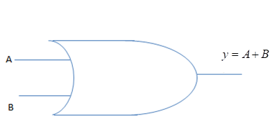
(b). Draw a logic symbol of OR gate.
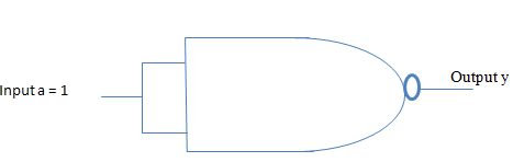
(c). Write the value of output y in the given circuit
(d). Write the name of the diode used in voltage regulation.
Answer
634.2k+ views
- Hint: In order to solve these types of questions we will use the concept of logic gates and take the help of truth tables of the gates. First we need to know what a logic gate is and for what they are used or where they are used.
Complete step-by-step answer:
(a). Logic gate- A logic gate is the basic building block of the digital system. It is the part of an electronic circuit which has more than one input and has a single output. Depending upon the relationship between the input and output logic gates are named as AND, OR and NOT.
As we know NAND gate is the combination of AND and NOT gate. NAND gate is called universal gate because with the help of NAND gate we can accomplish any basic operation. NOR gate is also a universal gate.
(b). The logic symbol of the OR gate is shown in the below figure.
(c). As from the truth table of NAND gate, we know that when both terminals of NAND are applied to the same input, the output of the NAND gate is zero.
(d). Zener diodes are always operated in reverse biased condition for voltage regulation.
Note: In order to solve problems related to logic circuits you need to have the concept of Boolean algebra i.e. the form of algebraic expression showing operation of the logic circuit. Truth table which defines the function of a logic gate by providing a concise list of input and output which shows all possible combinations.
Recently Updated Pages
Master Class 12 Business Studies: Engaging Questions & Answers for Success
Master Class 12 Chemistry: Engaging Questions & Answers for Success
Master Class 12 Biology: Engaging Questions & Answers for Success
Class 12 Question and Answer - Your Ultimate Solutions Guide
Master Class 11 English: Engaging Questions & Answers for Success
Master Class 11 Social Science: Engaging Questions & Answers for Success
Trending doubts
Which are the Top 10 Largest Countries of the World?
Draw a labelled sketch of the human eye class 12 physics CBSE
The end of compass needle which points towards north class 12 physics CBSE
Differentiate between homogeneous and heterogeneous class 12 chemistry CBSE
Why is the cell called the structural and functional class 12 biology CBSE
When was the first election held in India a 194748 class 12 sst CBSE