


Draw the circuit diagram of TTL NAND gate and explain its working with the help of a truth table.
Answer
592.8k+ views
Hint: Recall that NAND gate allows is only 0 when both inputs are equal to 1. A TTL NAND gate logic circuit has at least four bi polar junction transistors in which the input (transistor which receives input) has two emitters. The output is taken between the emitter and collector of two different transistors.
Complete answer:
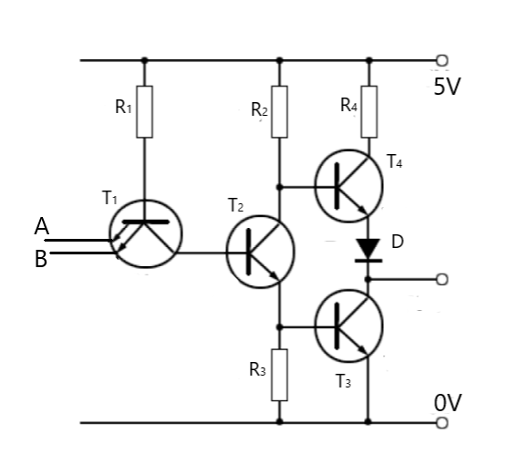
The above diagram is the circuit diagram of a TTL NAND gate.
From the diagram, we shall explain the working. Now, as seen, the transistor \[{T_1}\] has two emitters to allow two inputs into the transistor. Now, as connected the base voltage will be at 5V. if both inputs are logic 1 (usually means about 5V too), the potential difference across base and emitter would be zero or nearly. Hence, no current will flow and the transistor is turned off. So, the collector voltage would also be equal to about 5V. Hence, this potential can drive current through the emitter of the transistor \[{T_2}\]. This then will allow the collector voltage of the transistor \[{T_2}\] to fall.
Now due to the current flowing through the emitter, there would be a voltage drop across the resistor \[{R_3}\]. The desired voltage drop would be about \[0.7V\]. As seen, this is the input of the transistor \[{T_3}\]. Hence, the transistor is turned on. Due to saturation, the collector voltage will fall to about \[0.2V\] which is a logic 0. A
For the transistor \[{T_4}\], observe that the emitter voltage is made up of the entire voltage of the transistor \[{T_3}\] plus the voltage drop across the diode D about \[0.7V\]. Hence the emitter potential would be \[0.7 + 0.2 = 0.9V\]. Now the base voltage of the transistor \[{T_4}\], would be the voltage across the base-emitter of \[{T_3}\] and the voltage of the entire transistor (i.e.) voltage across emitter-collector. This would also be equal to about \[0.9V\]. Hence the emitter voltage and the collector voltage are equal. So the transistor \[{T_4}\] will be turned off too. So the output is zero when both inputs are 1.
Note:
For clarity, note that logic circuits are made such that the transistors will work in saturation mode. Hence, in the explanation above, note that when we say current is flowing, we imply that saturation current is flowing.
Complete answer:
The above diagram is the circuit diagram of a TTL NAND gate.
From the diagram, we shall explain the working. Now, as seen, the transistor \[{T_1}\] has two emitters to allow two inputs into the transistor. Now, as connected the base voltage will be at 5V. if both inputs are logic 1 (usually means about 5V too), the potential difference across base and emitter would be zero or nearly. Hence, no current will flow and the transistor is turned off. So, the collector voltage would also be equal to about 5V. Hence, this potential can drive current through the emitter of the transistor \[{T_2}\]. This then will allow the collector voltage of the transistor \[{T_2}\] to fall.
Now due to the current flowing through the emitter, there would be a voltage drop across the resistor \[{R_3}\]. The desired voltage drop would be about \[0.7V\]. As seen, this is the input of the transistor \[{T_3}\]. Hence, the transistor is turned on. Due to saturation, the collector voltage will fall to about \[0.2V\] which is a logic 0. A
For the transistor \[{T_4}\], observe that the emitter voltage is made up of the entire voltage of the transistor \[{T_3}\] plus the voltage drop across the diode D about \[0.7V\]. Hence the emitter potential would be \[0.7 + 0.2 = 0.9V\]. Now the base voltage of the transistor \[{T_4}\], would be the voltage across the base-emitter of \[{T_3}\] and the voltage of the entire transistor (i.e.) voltage across emitter-collector. This would also be equal to about \[0.9V\]. Hence the emitter voltage and the collector voltage are equal. So the transistor \[{T_4}\] will be turned off too. So the output is zero when both inputs are 1.
| A | B | Y |
| 0 | 0 | 1 |
| 0 | 1 | 1 |
| 1 | 0 | 1 |
| 1 | 1 | 0 |
Note:
For clarity, note that logic circuits are made such that the transistors will work in saturation mode. Hence, in the explanation above, note that when we say current is flowing, we imply that saturation current is flowing.
Recently Updated Pages
Master Class 12 Economics: Engaging Questions & Answers for Success
Master Class 12 Biology: Engaging Questions & Answers for Success
Master Class 11 English: Engaging Questions & Answers for Success
Master Class 11 Physics: Engaging Questions & Answers for Success
Master Class 11 Computer Science: Engaging Questions & Answers for Success
Master Class 11 Chemistry: Engaging Questions & Answers for Success
Trending doubts
Draw a labelled sketch of the human eye class 12 physics CBSE
Why is the cell called the structural and functional class 12 biology CBSE
Draw ray diagrams each showing i myopic eye and ii class 12 physics CBSE
Which are the Top 10 Largest Countries of the World?
Differentiate between homogeneous and heterogeneous class 12 chemistry CBSE
Which is the correct genotypic ratio of mendel dihybrid class 12 biology CBSE